Do you have a question about the Roland Va-3 and is the answer not in the manual?
Provides an introduction to the service notes for the VA-3.
Details the steps for disassembling the instrument.
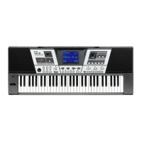
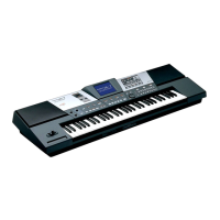
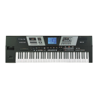
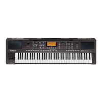
Details the keyboard action, number of keys, and control elements.
Describes the tone generation, PCM samples, and digital effects.
Outlines arranger features like styles, composer, and memories.
Covers the display type, user interface, and navigation methods.
Details the sequencer capabilities and data storage options.
Specifies the amplification power and available connections.
Lists power requirements, dimensions, weight, and included accessories.
Identifies and describes controls on the front panel.
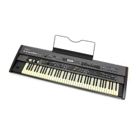
Details the connectors and ports located on the rear panel.
Illustrates the top-side internal components of the VA-3.
Provides a list of part numbers and descriptions.
Lists parts related to the instrument's casing and switches.
Details various sockets and connector parts.
Lists parts for the display and floppy disk drive units.
Lists integrated circuits, transistors, and diodes.
Details resistors, potentiometers, and capacitors.
Includes miscellaneous parts, inductors, crystals, and accessories.
Procedure for saving the system program and updating firmware.
How to display the current system program version.
Instructions for updating the system or test program via floppy disk.
Introduces the test mode and its structure.
Procedures for testing the LCD display and LEDs.
Tests for key scanning and touch screen functionality.
Details touch screen calibration and MIDI input/output testing.
Procedure for testing the instrument's flash memory.
Tests for ROM styles, RAM, and floppy disk drive.
Procedure for testing the audio output channels.
Instructions for calibrating the pitch bender.
How to enter the touch screen calibration mode.
Instructions for loading different language files.
Procedure for initializing the flash memory area.
Details of the right contact PCB assembly and its diagram.
Details of the left contact PCB assembly and its diagram.
Shows the main PCB assembly from component and solder sides.
Provides the overall circuit diagram for the main PCB.
Circuit diagrams for specific blocks of the main PCB.
Circuit diagrams for memory bank and FDC sections of the main PCB.
Circuit diagram for the LCD control section of the main PCB.
Shows the XPGS-4 PCB assembly from both sides.
First part of the circuit diagram for the XPGS-4 PCB.
Second part of the circuit diagram for the XPGS-4 PCB.
Details the LCD control PCB assembly and its circuit diagram.
Shows the Jack PCB assembly from the component side.
Details the D-Beam control PCB assembly and its circuit diagram.
Shows the main control PCB assembly from the component side.
Details the inverter PCB assembly and its circuit diagram.
Shows the Power & Amplifier PCB assembly from the component side.
| Keyboard | 61 keys with velocity sensitivity |
|---|---|
| Polyphony | 64 voices |
| Effects | Reverb, Chorus |
| Display | LCD |
| Connectivity | MIDI In/Out, Pedal |
| Power Supply | AC adapter (DC 9V) |