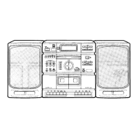
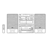
ICBLOCK DIAGRAM & DESCRIPTION
ICI 32 LB1 641 ( RECORD/PLAY SWITCHING)
PI
OUT 1
IN 1
GND
EEE5F’c.
IC101 CXA1782BQ ( SERVO SIGNAL PROCESSOR
I No. I Name I I / O I - Description
1 FEO o Focus error amplifier output.
2
FEI I Focus error input.
3
FDFCT I
Capacitor connection pin for detect time
constant.
4
FGD I
Ground this
pin through a capacitor when
decreasing the focus servo high-frequency
5
FLB I
External time constant setting
pin for increasing
the focus servo low frequency.
6
FEO
o
Focus drive output.
I 7 I FEM I 1 ] Focus amplifier negative input.
8
SRCH I
External time constant setting
pin for
generating focus servo waveform.
9
TGU I
External time constant setting pin
for switching
10
TG2 I
tracking high-frequency gain.
11 FSET I
High cut off frequency setting pin
for focus and
trackina r)hase compensation amriifier.
I 12 I
TAM I i I Trackina amDlifier neaative inout.
II
13 TAO
O I Tracking drive output.
14
SLP
I i ISled amplifier non-inverted input.
15 SLM I Sled amplifier negative input.
16
SLO o Sled drive output
17 ISET I
Setting pin
for Focus search, Tracking jump,
and Sled kick current.
18
Vcc -
+5.OV
I 19 I CLK I I ISerial data transfer clock irmut from CPU.
I
20 XLT [ I I Latch input from CPU.
21
I
DATA I I
I Serial data input from CPU.
22 XRST I Reset input resets at Low.
23
C.OUT o Track number count signal output.
24
SENS o
Outputs FZC, DFCT, TZC, gain, balance, and
others according to the command from CPU.
Input
output
I Action
IN IIIN2 10uTI10uT2 I
o 0 0 0
Ekake
1 0 1 0
Normai(Reverse)RoWy
o 1 0 1
Reverse(NrxmallF/o[&y
I
1 1 0 0
I
8rake
~
Input pin for the DEFECT bottom hold output
27
ccl I
DEFECT bottom hold output.
28 CB
I
Connection pin
for DEFECT bottom hold
capacitor.
29
m-
Connection pin for MIRR hold capacitor.
MIRR comparator non-inversed input.
I
30
RFI I
Input pin
for the RF summing amplifier output
capacitance-coupled.
31
RFO o
RF
summing amplifier output
Eve rrattern check Doint.
RF summing amplifier inverted input.
32
RFM I
The
RF amplifier gain is determined by the
resistance connected
between this pin and
RFO pin.
33 LD -
0 APC (Auto Power Control) amplifier output.
34
PHD I APC (Auto Power Control) amplifier input.
~
35
PHD1 I
36
PHD2 I
RF I-V amplifier inverted input.
37
FEBIAS I
Bias adjustment
of focus error amplifier.
38
F I
F I-V and
E I-V amplifier inverted input.
39
E I
40
Ell -
I-V amplifier
E gain adjustment.
I
41
v~~ - GND
42 TEO
o Tracking error amplifier output.
43 LPFI I
Comparator inr.wt for balance adjustment.
44 TEI
Ill
Tracking error input.
45 ATSC I
Window comparator input for
ATSC detection.
J
46
TZC
I
Tracking zero-cross comparator input.
48
Vc
o (Vcc+VEE)12
DC voltage output.
-46-
 Loading...