Barracuda 18XL Product Manual, Rev. A 81
Note.
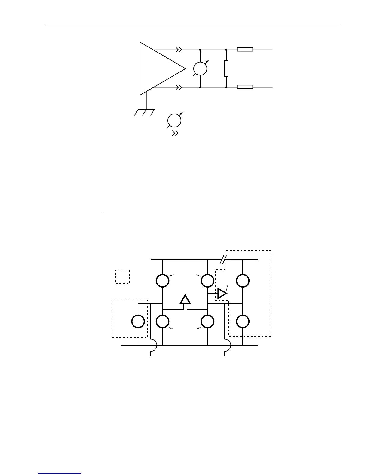
Resistors are ± 0.1%
Figure 13. LVD steady-state output voltage test circuit (T10/1302D, Annex A, Figure 1)
Input characteristics
Each signal (Vs) received by LVD interface receiver circuits shall have the following input characteristics when
measured at the disk drive connector:
Steady state Low level output voltage* = 0.030 V = < V
s
= < 3.6 V (signal negation/logic 0)
Steady state High level output voltage* = –3.6 V = < V
s
= < –0.030 V (signal assertion/logic 1)
Differential voltage = +
0.30 V minimum with common-mode voltage ranges 0.700 V = < V
cm
= < 1.800 V. (T10/
1302D, SPI-3)
*These voltages shall be measured between the output terminal and the SCSI device’s logic ground reference.
Input characteristics shall additionally conform to EIA RS-485-983.
Figure 14. Typical SE-LVD alternative transmitter receiver circuits
V1
–SIGNAL
100Ω
V2
+SIGNAL
MEASURED
PARAMETER
STEADY STATE
LOGIC INPUT
(1 OR 0)
DEVICE CONNECTOR
100Ω
75Ω
V
s
D
VCCA VCCB
Single
Ended
Circuitry
Single
Ended
Receiver
Single
Ended
Negation
Driver
Single
Ended
Assertion
Driver
Single
Ended
Ground
Driver
Single Ended:
LVD:
LVD Signal Drivers
LVD Signal Drivers
LVD
Receiver
Ground
GND
+Signal
–Signal
–Signal