AUDIO_EN/DISbPin _ctrl7
TP18
Y1 CS10-27.000M
C43 16p
C44 16p
IOPROC_EN/D ISbPin _ctrl6
A_GND
C18
22u
VID_DAT_Out4
JTAG/HOSTbPin _ctrl0
20BIT/10BITbPin _ctrl5
RESET
A_GND
C9
1u
12. Impedance controlled signals (refer to PCB layout guide).
Floating or +3.3V or GND
SDO_EN/DISbPin _ctrl4
RESET
8. Lable the connectors, LEDs, DIP sw itches and jumpers. Lable s ome critical signals on the connectors;
RC_BYbPin _ctrl3
VID_DAT_Out18
VID_DAT_Out3
R21
DNP
FW_ENPin _ctrl2
A_GND
STANDBYPin _ctrl1
VID_DAT_Out[ 19:0]
A_GND
R7
105R
VID_DAT_Out17
IO_VDD
+1.2VA
VID_DAT_Out2
4. SQT and TMM series connectors are rated for 3A f rom 20C-80C, w ith operation temp range of -65-+125C
PCLK
R19
DNP
Close to GS2971
1
2
3
4
5
6
7
89
10
11
12
13
14
15
16
RN2 742C163220
HVF[2:0]
VID_DAT_Out16
C101
470n
C100
470n
VID_DAT_Out1
+3.3VA
Data Error
AUDIO_Out [6: 0]
VID_DAT_Out15
Pin _ctrl[10:0]
VBG
A1
LF
A2
LB_CONT
A3
VCO_VDD
A4
STAT0
A5
STAT1
A6
STAT2
B5
STAT3
B6
STAT4
C5
STAT5
C6
IO_VDD
A7
PCLK
A8
DOUT0
K8
DOUT1
J8
DOUT2
K9
DOUT3
K10
DOUT4
J9
DOUT5
J10
DOUT6
H9
DOUT7
H10
DOUT8
F9
DOUT9
F10
DOUT10
E9
DOUT11
E10
DOUT12
C8
DOUT13
C10
DOUT14
C9
DOUT15
B10
DOUT16
B9
DOUT17
A10
DOUT18
A9
DOUT19
B8
A_VDD
B1
PLL_VDD
B2
A_TEST
B3
VCO_GND
B4
IO_GND
B7
SDI
C1
A_GND
C2
PLL_VDD
C3
PLL_VDD
C4
RESET
C7
SDI
D1
A_GND
D2
A_GND
D3
PLL_GND
D4
CORE_GND
D5
CORE_VDD
D6
SW_EN
D7
JTAG/HOST
D8
IO_GND
D9
IO_VDD
D10
SDI_VDD
E1
A_GND
E3
PLL_GND
E4
CORE_GND
E5
CORE_VDD
E6
SDOUT_TDO
E7
SDIN_TDI
E8
AGC+
F1
RSV
F2
A_GND
F3
PLL_GND
F4
CORE_GND
F5
CORE_VDD
F6
CS_TMS
F7
SCLK_TCK
F8
AGC-
G1
A_GND
G2
RC_BYP
G3
CORE_GND
G4
CORE_GND
G5
CORE_VDD
G6
SMPTE_BYPASS
G7
DVB_ASI
G8
IO_GND
G9
IO_VDD
G10
BUF_VDD
H1
BUF_GND
H2
AUDIO_EN/DIS
H3
WCLK
H4
TIM_861
H5
XTA L _O U T
H6
20BIT/10BIT
H7
IOPROC_EN/D IS
H8
SDO
J1
SDO_EN/DIS
J2
AOUT_1/2
J3
ACLK
J4
AOUT_5/6
J5
XTA L 2
J6
IO_GND
J7
SDO
K1
STANDBY
K2
AOUT_3/4
K3
AMCLK
K4
AOUT_7/8
K5
XTA L 1
K6
IO_VDD
K7
SDI_GND
E2
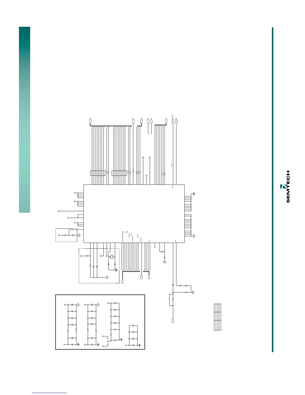
U5
GS2971
Close to GS2971
Lock
VID_DAT_Out0
WCLK AUDIO_Out 0
R37 22R
ACLK AUDIO_Out 1
R38 22R
+1.2V
5. IO_V DD can be +3.3V, w hich is s upplied by this board through a 1-ohm jumper, or dif fer ent
voltage supplied by the output board connected to it, in w hich case the 1-ohm jumper shall be removed;
R24 22R
R25 22R
VID_DAT_Out14
10. Analog pow er and ground isolation (refer to PCB layout guide).
9. Minimum of 3x trace w idth spacing f or DOUT10~19 , PCLK;
11. Critital 3G signal layout (ref er to PCB layout guide);
SCLKGSPI1
SDINGSPI2
SDOUTGSPI3
CS0GSPI0
Lock
+3.3VA
Data Error
C51
1u
R42 75R
L3 6n2
R45
75R
R46
37R4
C49
1u
A_GND
VID_DAT_Out13
VID_DAT_Out11
GS2971 Power Decoupling & Filtering
VID_DAT_Out12
VID_DAT_Out10
1
2
3
JP7
TP7
7. Us e BNC ground as the ground test points;
VCC_1.8V
TP19
VID_DAT_Out9
+3.3VA
GSPI[3:0]
PCLK
R18 22R
C26
1u
TP20
13. Via size test points should be as close as pos s ible to the pins;
AOUT_3/4 AUDIO_Out 4
AOUT_1/2 AUDIO_Out 5
VID_DAT_Out8
6. The value of the serial resistors on video output port w ill be determined by board signal integrity test;
R16 22R
R17 22R
R14 22R
FHVF2
VHVF1
H
HVF0
GND
C25
1u
TP8
Lock
GND
AOUT_7/8 AUDIO_Out 2
AOUT_5/6 AUDIO_Out 3
1
2
3
4
5
6
7
89
10
11
12
13
14
15
16
RN1 742C163220
VID_DAT_Out7
C31
1u
C34
10n
C17
10n
C27
10n
C16
10n
C41 47n-470n
C15
10n
R12
0R
R10
0R
C30
10n
R2
0R
C14
10n
C29
10n
C8
10n
R91
0R
C24
10n
C33
10n
R11
0R
C13
10n
C35
10n
C12
10n
C32
10n
+1.2VA
C28
10n
C11
10n
A_GND
A_GND
VCC_3.3V
GND
GND
VCC_3.3V
+1.2V
GND
GND
+1.2VA
+3.3VA
IO_VDD
+1.2V
R20 22R
TIM861Pin _ctrl10
VID_DAT_Out6
LB_CONT Settings:
VID_DAT_Out19
Data Error
R22 22R
SMPTE_BYPASSbPin _ctrl9
AMCLK AUDIO_Out 6
3. Pow er consumption:
2. DNP (Do Not Populate);
217
+1.2V +3.3V
75GS2970_1
Notes:
Device
0GS2978 51
SDI Input
C42 1u
1. This board is GS2960/1 compatible;
217mATot al 191mA
C10
1u
DVB_ASIPin _ctrl8
VID_DAT_Out5
SDO
SDO
SDO
SDO