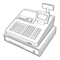
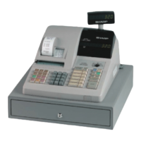
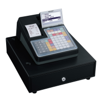
ER-A410/ER-A420 HARDWARE DESCRIPTION
– 14 –
12. PRINT RATIO LIMITATION
Max. 288dot/1line x 140line (Corresponds to black background LOGO
print.)
Ave. 108dot/1line or less (Corresponds to 12.5% of all dots.)
13. BUZZER
A buzzer of piezo type is used.
The oscillation frequency is 4.0kHz m 0.5kHz.
14. RESET
The RESET signal is generated under the following condition.
1) When the MODE KEY SWITCH is moved from SRV’ to another
position (except for OFF).
15. POFF
The POFF signal is changed from 0 to 1 when the 5V system power
and the 24V system power reach the operating voltage. When they fall
below the operating voltage, the signal is changed from 1 to 0.
POFF, RESET TIMING CHART
16. I/O
<LED Segment Signal> Write
<Serial I/O ch2 receive signal> Read
<LCD Write Data> Write
<Key Return Signal, Key Exchange Signal> Read
<LCD Read Data> Read
<LCD Control Signal/Key Strobe Signal> Write
<Key Return Signal> Read
<LCD Control Signal/Key Strobe Signal> Write
<EFT Data> Write/Read
<EFT Status> Read
+5V
+24V
RESET
POFF
EFTRES
20.8V
POWER ON Instant service
interruption
MODE
SRV'
MODE
Other than
SRV'
POWER OFF
Address Bit7 Bit6 Bit5 Bit4 Bit3 Bit2 Bit1 Bit0
04000h dp g f e d c B a
Address Bit7 Bit6 Bit5 Bit4 Bit3 Bit2 Bit1 Bit0
04000h X X X X /CD2 /DR2 /CS2 /CI2
Address Bit7 Bit6 Bit5 Bit4 Bit3 Bit2 Bit1 Bit0
04001h DB7 DB6 DB5 DB4 DB3 DB2 DB1 DB0
Address Bit7 Bit6 Bit5 Bit4 Bit3 Bit2 Bit1 Bit0
04001h X X X X KR11 KR10 KR9 KR8
Address Bit7 Bit6 Bit5 Bit4 Bit3 Bit2 Bit1 Bit0
04002h DB7 DB6 DB5 DB4 DB3 DB2 DB1 DB0
Address Bit7 Bit6 Bit5 Bit4 Bit3 Bit2 Bit1 Bit0
04003h X E R/W RS KS3 KS2 KS1 KS0
Address Bit7 Bit6 Bit5 Bit4 Bit3 Bit2 Bit1 Bit0
04003h KR7 KR6 KR5 KR4 KR3 KR2 KR1 KR0
Address Bit7 Bit6 Bit5 Bit4 Bit3 Bit2 Bit1 Bit0
04003h X E R/W RS KS3 KS2 KS1 KS0
Address Bit7 Bit6 Bit5 Bit4 Bit3 Bit2 Bit1 Bit0
0400Eh D7 D6 D5 D4 D3 D2 D1 D0
Address Bit7 Bit6 Bit5 Bit4 Bit3 Bit2 Bit1 Bit0
0400Fh X XXXXCLMIBFOBF