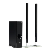
HT-DV40H
8 – 38
IC11 VHILC750512-1 : AUDIO ENHANCER ( LC750512 ) ( 1/2 )
PIN DESCRIPTION
Pin No. Terminal Name Input / Output Function
1 PLLPWRR Input Power ring for PLL (ESD) (+1.8 V).
2 PLLGNDR — GND for PLL (ESD).
3 PLLAVDD Input Power supply for PLL (+1.8 V).
4 PLLAVSS — GND for PLL.
5 PLLDVDD Input Digital power supply for PLL (+1.8 V).
6 PLLDVSS — Digital GND for PLL (ESD).
7 TEST2 Input Test terminal.
8 TEST3 Input Test terminal.
9 DVSS4 — Digital GND.
10 DVDD4 Input Digital power supply (+1.8 V).
11 XVSS — GND for crystal.
12 XOUT Output Crystal oscillating output.
13 XIN Input Crystal oscillating input.
14 XVDD Input Power supply for crystal (+3.3 V).
15 CVDD4 Input Digital power supply (+3.3 V).
16 CVSS4 — Digital GND.
17 TEST0 Input Test terminal.
18 TEST1 Input Test terminal.
19 TEST4 Input Test terminal.
20 TEST5 Input Test terminal.
21 BVSS1 — Logic GND in analog chip.
22 BVDD1 Input Logic power supply in analog chip (+3.3 V).
23 AVSS4 — DAC analog GND.
24 AVDD4 Input DAC analog VDD (+5 V).
25 AVDD3 Input EVR analog VDD (+5 V).
26 AVSS3 — EVR analog GND.
27 AOUT1 Output Lch EVR output.
28 EVRINL Input Lch EVR input.
29 DAOUTL Output Lch DAC analog output.
30 DAOUTR Output Rch DAC analog output.
31 EVRINR Input Rch EVR input.
32 AOUT2 Output Rch EVR output.
33 AVSS2 — GND for VREF.
34 AVDD2 Input VDD for VREF (+5 V).
35 VREF2 Output Reference voltage output terminal 2 (DAC, EVR).
36 VREF1 Output Reference voltage output terminal 1 (ADC).
37 INL Input Lch ADC analog input.
38 INR Input Rch ADC analog input.
39 AVSS1 — ADC analog GND.
40 AVDD1 Input ADC analog power supply (+5V)
41* TEST6 Input/Output Test terminal.
42 XSEL0 Input/Output Crystal frequency setting signal 0.
43 XSEL1 Input/Output Crystal frequency setting signal 1.
44 XSEL2 Input/Output Crystal frequency setting signal 2.
45 CVSS1 — Digital GND.
46 CVDD1 Input Digital power supply (+3.3 V).
47 LRCKI Input LR clock input.
48 BCKI Input Bit clock input.
49 DATAI Input Data input.
50 SCKII — External clock input.
51 DVSS1 — Digital GND.
52 DVDD1 Input Digital power supply (+1.8V).
53* SCKO Output DAC master clock output.
54 TEST7 Input Test terminal.
55* DATAO2 Output Data output 2.
56* DATAO1 Output Data output 1.
57* DATAO0 Output Data output 0.
58* BCKO Output Bit clock output.
59* LRCKO Output LR clock output.
60 CVSS2 — Digital GND.
61 CVDD2 Input Digital power supply (+3.3 V).
62 XPDESC Input DSP power down release signal (L-Active).
63* PDEN Output DSP power down signal (H-Active).
64 DVSS2 — Digital GND.