119
LC-26GA5E
LC-32GA5E
LC-26GA5E
LC-32GA5E
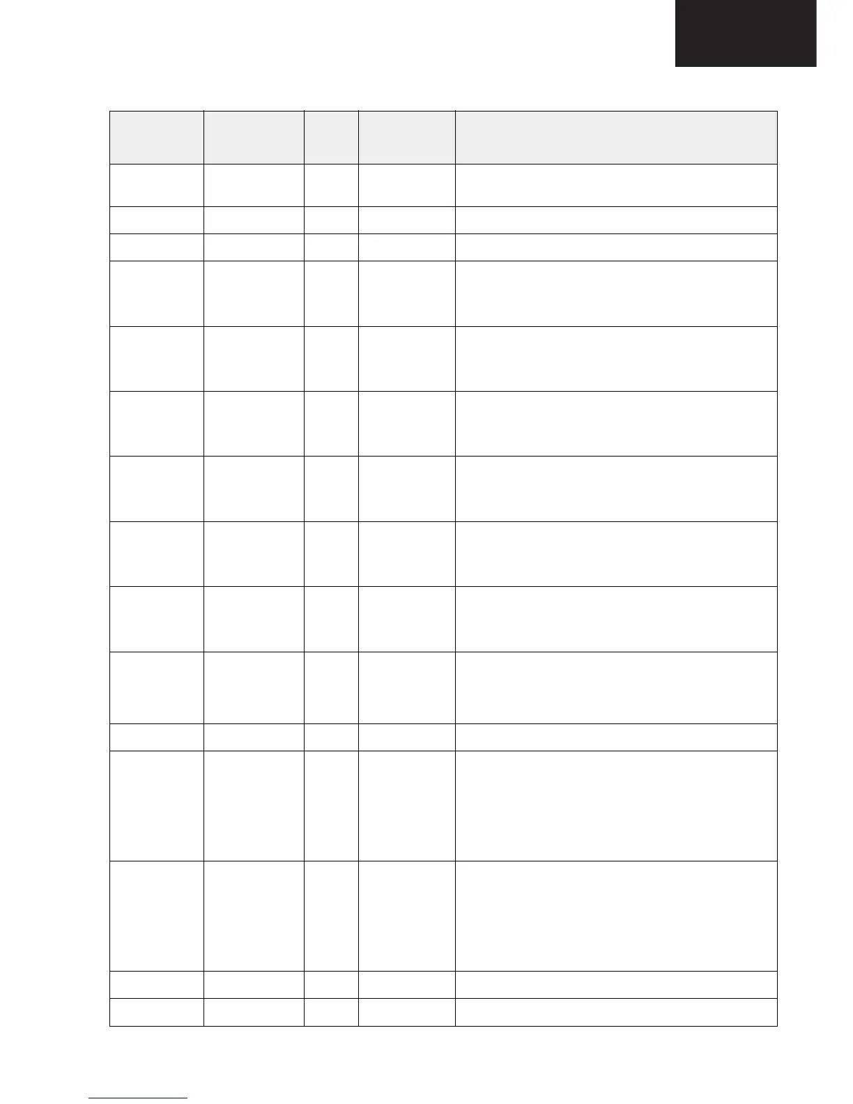
4.3. Description of Pins IC6004, continued
24 XOUT O LV (pull
down)
Crystal connection 2
25 VSSP1 S Supply digital pad (0 V)
26 VDDP1 S Suplly digital pad (3.3 V)
27 RGBOUT9 O LV Tristate (SELOMODE=0)
Digital (red: SELRB=0; blue: SELRB=1;)
Output [MSB](SELOMODE=1)
28 RGBOUT8 O LV Tristate (SELOMODE=0)
Digital (red: SELRB=0; blue: SELRB=1;)
Output (SELOMODE=1)
29 RGBOUT7 O LV Tristate (SELOMODE=0)
Digital (red: SELRB=0; blue: SELRB=1;)
Output (SELOMODE=1)
30 RGBOUT6 O LV Tristate (SELOMODE=0)
Digital (red: SELRB=0; blue: SELRB=1;)
Output (SELOMODE=1)
31 RGBOUT5 O LV Tristate (SELOMODE=0)
Digital (red: SELRB=0; blue: SELRB=1;)
output (SELOMODE=1)
32 RGBOUT4 O LV Tristate (SELOMODE=0)
Digital (red: SELRB=0; blue: SELRB=1;)
Output (SELOMODE=1)
33 AVO/ITR O LV Active video output (CPUIRQ=0)
Interrupt signal output from μC (CPUIRQ=1)
Static 0 (CPUIRQ=2)
Static 1 (CPUIRQ=3)
34 VOUT O LV Vertical sync output
35 HOUT O LV Horizontal sync output.
(Synchronized to 40.5-81 MHz CLKOUTSEL72=1)
(Synchronized to 20.25-40.5 MHz
CLKOUTSEL72=0 and CLKOUTSEL=1)
(Synchronized to 15.1875-30.75 MHz
CLKOUTSEL72=0 and CLKOUTSEL=0)
36 CLKOUT O LV Output clock disabled (CLKOUTON=0)
Output clock (max. 81 MHz) (CLKOUT=1)
(40.5-81 MHz CLKOUT72=1
20.25-40.5 MHz CLKOUT72=0 and CLKOUTSEL=1
1515.1875-30.37 MHz CLKOUT72=0 and
CLKOUTSEL=0)
37 VSSP2 S Supply digital pad (0 V)
38 VDDP2 S Supply digital pad (3.3 V)
Pin No. Pin Name Type Connection
(If not used)
Short Description
PMQFP144-4