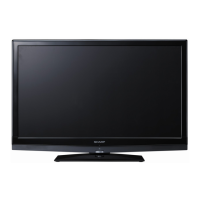
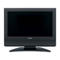
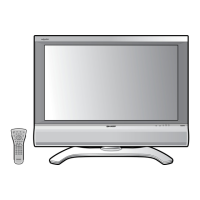
LC-26SB25E/S/RU, LC-32SB25E/S/RU, LC-42SB55E/S/RU
62
2.3. U104 (L5985 VFQFPN8)
2.3.1 Pin Connections and short description
N°
Type Description
1
OUT Regulator output
2
SYNCH Master/Slave Synchronization. When it is left floating, a signal with a phase shift of half a period respect to the power turn
on is present at the pin. When connected to an external signal at a frequency higher than the internal one, then the
device is synchronized by the external signal, with zero phase shift.
Connecting together the SYNC pin of two devices, the one with higher frequency works as master and the other one as
slave; so the two power turn on have a phase shift of half a period.
3
INH A logical signal (active high) disable the device. With INH higher than 1.9V the device is OFF and with INH lower than
0.6V the device is ON.
4
COMP Error Amplifier output to be used for loop frequency compensation
5
FB Feedback input. Connecting the output voltage directly to this pin the output voltage is regulated at 0.6V. To have higher
regulated voltages an external resistor divider is required from Vout to FB pin.
6
F
SW
The switching frequency can be increased connecting an external resistor from FSW pin and ground. If this pin is left
floating the deice works at its free-running frequency of 250KHz.
7
GND Ground
8
V
CC
Unregulated DC input voltage
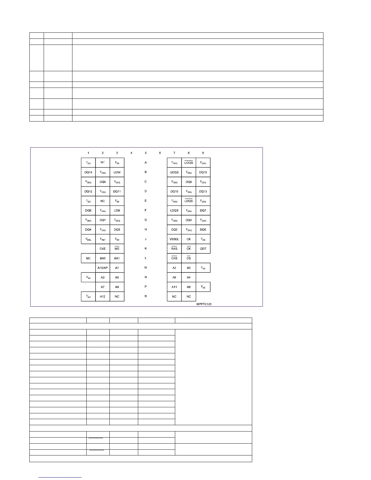
2.4. U351 (HYB18TC256160BF-3S TFBGA-84-55)
2.4.1 Pin Connections and short description
Ball#/Pin# Name Pin Type Buffer Type Function
Data Signals ×16 Organization
G8
DQ0 I/O SSTL
G2
DQ1 I/O SSTL
H7
DQ2 I/O SSTL
H3
DQ3 I/O SSTL
H1 DQ4 I/O SSTL
H9 DQ5 I/O SSTL
F1 DQ6 I/O SSTL
F9 DQ7 I/O SSTL
C8 DQ8 I/O SSTL
C2 DQ9 I/O SSTL
D7 DQ10 I/O SSTL
D3 DQ11 I/O SSTL
D1 DQ12 I/O SSTL
D9 DQ13 I/O SSTL
B1 DQ14 I/O SSTL
B9 DQ15 I/O SSTL
Data Signal 15:0
Data Strobe ×16 Organization
B7 UDQS
I/O SSTL
A8
UDQS
I/O SSTL
Data Strobe Upper Byte
F7
LDQS
I/O SSTL
E8
LDQS
I/O SSTL
Data Strobe Lower Byte
Data Mask ×16 Organization
 Loading...