LC-32DH57E-BK/RU-BK/S-BK
5 – 5
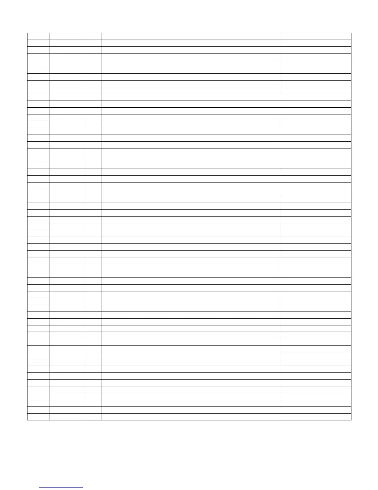
2.2.2 Pin Connections and short description
Pin No. Pin Name I/O Pin Function sheet name
1 AIN8R I Channel 8 right input. open
2 AIN8L I Channel 8 left input. open
3 MVDD33 — Multiplexer positive supply 3.3 voltage. —
4 VCM33 O Multiplexer midrail divider decoupling pin. C-GND
5 MGND33 — Multiplexer negative supply. GND
6 ADCOUTL O Analog multiplexer left output. AUDIO_IN_L
7 ADCOUTR O Analog multiplexer right output. AUDIO_IN_R
8 HPOUTL O Headphone right channel output. HP_L
9 HPGND — Headphone ground supply pin. GND
10 HPVDD — Headphone power supply pin. S9V
11 HPOUTR O Headphone right channel output. HP_R
12 AGND — Analog negative supply. GND
13 PGA0OUTL O PGA channel 0 left output. open
14 PGA0OUTR O PGA channel 0 right output. open
15 AVDD — Analog positive supply 12 voltage or 9 voltage. S9V
16 VCMPGA O PGA midrail divider decoupling pin. C-GND
17 PGA2OUTL O PGA channel 2 left output. SPK_OUT_L
18 PGA2OUTR O PGA channel 2 right output. SPK_OUT_R
19 PGA1OUTL O PGA channel 1 left output. MONITOR_L
20 PGA1OUTR O PGA channel 1 right output. MONITOR_R
21 INPUT2R I Channel 2 right input to PGA gain module. AOUT_SP_R
22 INPUT2L I Channel 2 left input to PGA gain module. AOUT_SP_L
23 INPUT0R I Channel 0 right input to PGA gain module. AOUT_HP_R
24 INPUT0L I Channel 0 left input to PGA gain module. AOUT_HP_L
25 INPUT1R I Channel 1 right input to PGA gain module. AOUT_MONI_R
26 INPUT1L I Channel 1 left input to PGA gain module. AOUT_MONI_L
27 CL I Control clock pin in serial mode. SCLO_400K
28 DI I/O Control data pin in serial mode. SDAO_400K
29 MUTE# I Hardware mute function when this pin is driven low. AUSW_MUTE
30 RESET# I The device enters a low power mode when this pin is driven low. AUSW_RST
31 GPIO0 I General Purpose I/O 0 and also shares hardware trapped function. R-GND
32 GPIO1 I General Purpose I/O 1. open
33 GPIO2 I General Purpose I/O 2. open
34 GPIO3 I General Purpose I/O 3. COMP_PLUG
35 GPIO4 I General Purpose I/O 4. MUTE_A_ALL
36 DVDD — Digital positive supply 3.3 voltage. D3.3V
37 DGND — Digital negative supply. ground
38 GPIO5 I General Purpose I/O 5. open
39 GPIO6 I General Purpose I/O 6. open
40 GPIO7 I General Purpose I/O 7. TUNER_OUT_SEL
41 GPIO8 I General Purpose I/O 8. TUNER_OUT_CVBS_MUTE
42 GPI I Only General Purpose Input and support internal digital scan mode. CVBS_PLUG
43 AIN1R I Channel 1 right input (default). SC1_IN_R
44 AIN1L I Channel 1 left input (default). SC1_IN_L
45 AIN2R I Channel 2 right input. SC2_IN_R
46 AIN2L I Channel 2 left input. SC2_IN_L
47 AIN3R I Channel 3 right input. COMP_IN_R
48 AIN3L I Channel 3 left input. COMP_IN_L
49 AIN4R I Channel 4 right input. RC/HDMI_IN_R
50 AIN4L I Channel 4 left input. RC/HDMI_IN_L
51 AIN5R I Channel 5 right input. CVBS_IN_R
52 AIN5L I Channel 5 left input. CVBS_IN_L
53 AIN6R I Channel 6 right input. open
54 AIN6L I Channel 6 left input. open
55 AIN7R I Channel 7 right input. open
56 AIN7L I Channel 7 left input. open