LC-32DH57E-BK/RU-BK/S-BK
5 – 14
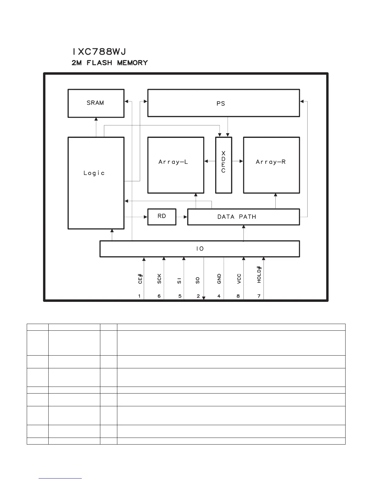
2.9. IC8403 (RH-iXC788WJZZY)
2.9.1 Block Diagram
2.9.2 Pin Connections and short description
Pin No. Pin Name I/O Pin Function
1CS#
(Chip Select)
I Places device in active power mode when driven low.
Deselects device and places SO at high impedance when high.
After power-up, device requires a falling edge on CS# before any command is written.
Device is in standby mode when a program, erase, or Write Status Register operation is not in progress.
2SO
(Signal data Output)
O Transfers data serially out of the device on the falling edge of SCK.
3W#
(Write Protect)
I Protects the memory area specified by Status Register bits BP2:BP0.
When driven low, prevents any program or erase command from altering the data in the protected mem-
ory area.
4 GND — Ground
5SI
(Serial Data Input)
I Transfers data serially into the device. Device latches commands, addresses, and
program data on SI on the rising edge of SCK.
6SCK
(Serial Clock)
I Provides serial interface timing.
Latches commands, addresses, and data on SI on rising edge of SCK.
Triggers output on SO after the falling edge of SCK.
7 HOLD# I Pauses any serial communication with the device without deselecting it. When driven low, SO is at high
impedance, and all input at SI and SCK are ignored. Requires that CS# also be driven low.
8 VCC — Supply Voltage