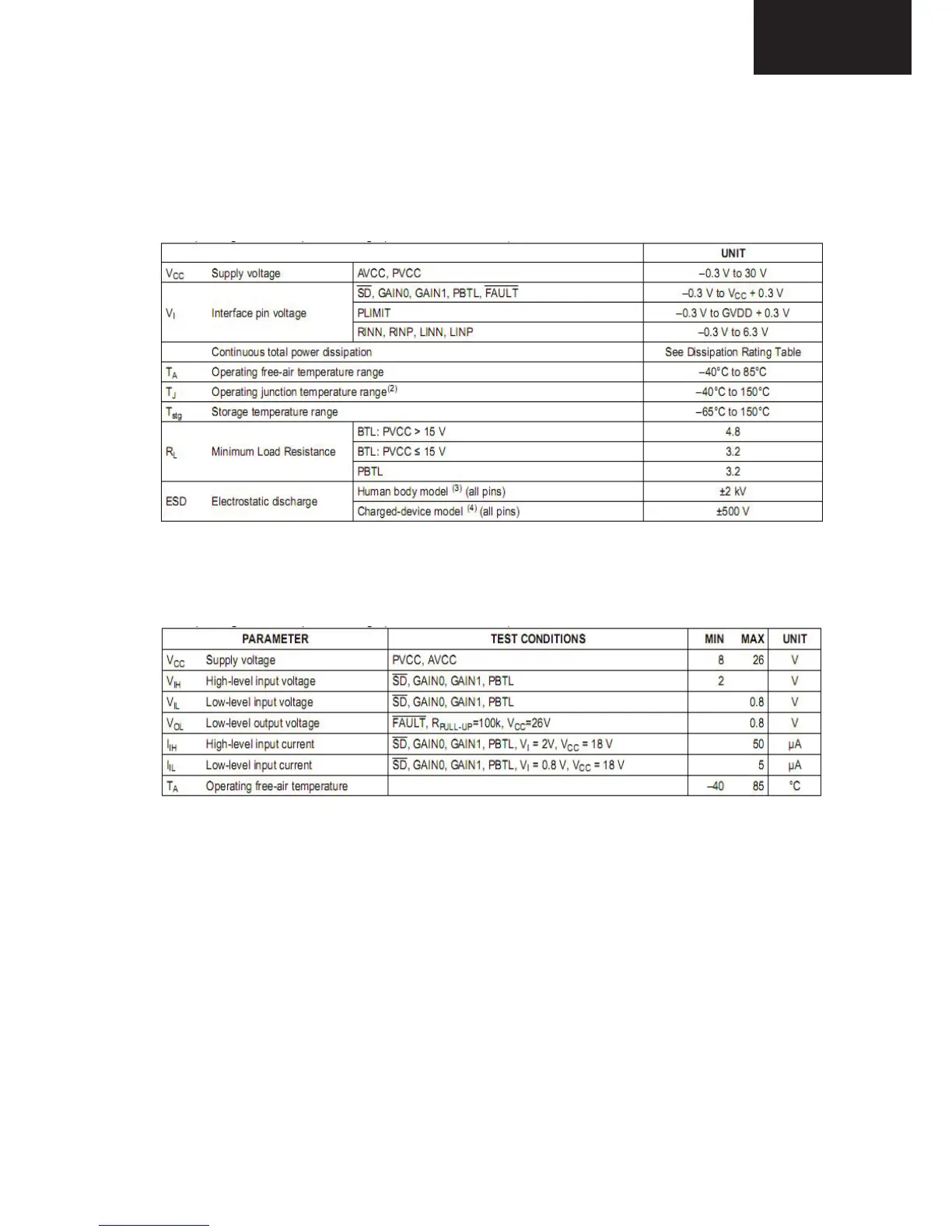
7
The TPA3110D2 can drive stereo speakers as low as 4 7KHKLJKHIILFLHQFy of the
TPA3110D2, 90%, eliminates the need for an external heat sink when playing music. The
outputs are also fully protected against shorts to GND, VCC, and output-to-output. The short-
circuit protection and thermal protection includes an auto-recovery feature.
b. Features
• 15-W/ch into an 8-/RDGVDW7+'1)URPD-V Supply
• 10-W/ch into 8-/RDGVDW7+'1)URPD 13-V Supply
• 30-W into a 4-0RQR/RDGDW7+'1)URPD-V Supply
• 90% Efficient Class-D Operation Eliminates Need for Heat Sinks
• Wide Supply Voltage Range Allows Operation from 8 V to 26 V
• Filter-Free Operation
• SpeakerGuard™ Speaker Protection Includes Adjustable Power Limiter plus DC Protection
• Flow Through Pin Out Facilitates Easy Board Layout
• Robust Pin-to-Pin Short Circuit Protection and Thermal Protection with Auto Recovery
Option
• Excellent THD+N / Pop-Free Performance
• Four Selectable, Fixed Gain Settings
• Differential Inputs
e. Pin Functions
.
PIN
I/O/P DESCRIPTION
Pin
NAME
Number
Shutdown logic input for audio amp (LOW = outputs Hi-Z, HIGH = outputs
SD
1 I
enabled). TTL logic levels with compliance to AVCC.
Open drain output used to display short circuit or dc detect fault status. Voltage
compliant to AVCC. Short circuit faults can be set to auto-recovery by connecting
FAULT
2 O
FAULT pin to SD pin. Otherwise, both short circuit faults and dc detect faults must
be reset by
cycling
PVCC.
LINP 3 I
Positive audio input for left channel. Biased at 3V.
LINN 4 I Negative audio input for left channel. Biased at 3V.
GAIN0 5 I
Gain select least significant bit. TTL logic levels with compliance to AVCC.
GAIN1 6 I
Gain select most significant bit. TTL logic levels with compliance to AVCC.
AVCC 7 P
Analog supply
AGND 8 Analog signal ground. Connect to the thermal pad.
High-side
FET gate drive supply. Nominal voltage is 7V. Also should be used as
GVDD
9 O
supply for PLIMIT function
Power limit level adjust. Connect a resistor divider from GVDD to GND to set
PLIMIT 10 I
power limit. Connect directly to GVDD for no power limit.
RINN 11 I
Negative audio input for right channel. Biased at 3V.
RINP 12 I
Positive audio input for right channel. Biased at 3V.
NC 13
Not connected
PBTL 14 I
Parallel BTL mode switch
Power supply for right channel H-bridge. Right channel and left channel power
PVCCR 15 P
supply inputs are connect internally.
Power supply for right channel H-bridge. Right channel and left channel power
PVCCR 16 P
supply inputs are connect internally.
BSPR 17 I
Bootstrap I/O for right channel, positive high-side FET.
OUTPR 18 O
Class-D H-bridge positive output for right channel.
PGND 19 Power ground for the H-bridges.
OUTNR 20 O
Class-D H-bridge negative output for right channel.
BSNR 21 I
Bootstrap I/O for right channel, negative high-side FET.
BSNL 22 I
Bootstrap I/O for left channel, negative high-side FET.
OUTNL 23 O
Class-D H-bridge negative output for left channel.
PGND 24
Power ground for the H-bridges.
OUTPL 25 O
Class-D H-bridge positive output for left channel.
BSPL 26 I
Bootstrap I/O for left channel, positive high-side FET.
Power supply for left channel H-bridge. Right channel and left channel power
PVCCL 27 P
supply inputs are connect internally.
Power supply for left channel H-bridge.
Right channel and left channel power
PVCCL 28 P
supply inputs are connect internally.
Copyright © 2009, Texas Instruments Incorporated Submit Documentation Feedback 5