11. 128Mbit NAND Flash Memory (U17)
ST NAND128-A
a) Key Features
Ŷ+,*+'(16,7<1$1')/$6+
MEMORIES
– Up to 1 Gbit memory array
– Up to 32 Mbit spare area
– Cost effective solutions for mass storage
applications
Ŷ1$1',17(5)$&(
– x8 or x16 bus width
– Multiplexed Address/ Data
– Pinout compatibility for all densities
Ŷ6833/<92/7$*(
– 1.8V device: VDD = 1.7 to 1.95V
– 3.0V device: VDD = 2.7 to 3.6V
Ŷ3$*(6,=(
– x8 device: (512 + 16 spare) Bytes
– x16 device: (256 + 8 spare) Words
Ŷ%/2&.6,=(
– x8 device: (16K + 512 spare) Bytes
– x16 device: (8K + 256 spare) Words
Ŷ3$*(5($'352*5$0
– Random access: 12µs (max)
– Sequential access: 50ns (min)
– Page program time: 200µs (typ)
Ŷ&23<%$&.352*5$002'(
– Fast page copy without external
buffering
Ŷ)$67%/2&.(5$6(
– Block erase time: 2ms (Typ)
Ŷ67$7865(*,67(5
Ŷ(/(&7521,&6,*1$785(
Ŷ&+,3(1$%/(µ'21¶7&$5(
OPTION
– Simple interface with microcontroller
Ŷ6(5,$/180%(5237,21
Ŷ+$5':$5('$7$3527(&7,21
– Program/Erase locked during Power
Transitions
Ŷ'$7$,17(*5,7<
– 100,000 Program/Erase cycles
– 10 years Data Retention
Ŷ5R+6&203/,$1&(
– Lead-Free Components are Compliant
with the RoHS Directive
Ŷ'(9(/230(17722/6
– Error Correction Code software and
hardware models
– Bad Blocks Management and Wear
Leveling algorithms
– File System OS Native reference
software
– Hardware simulation models
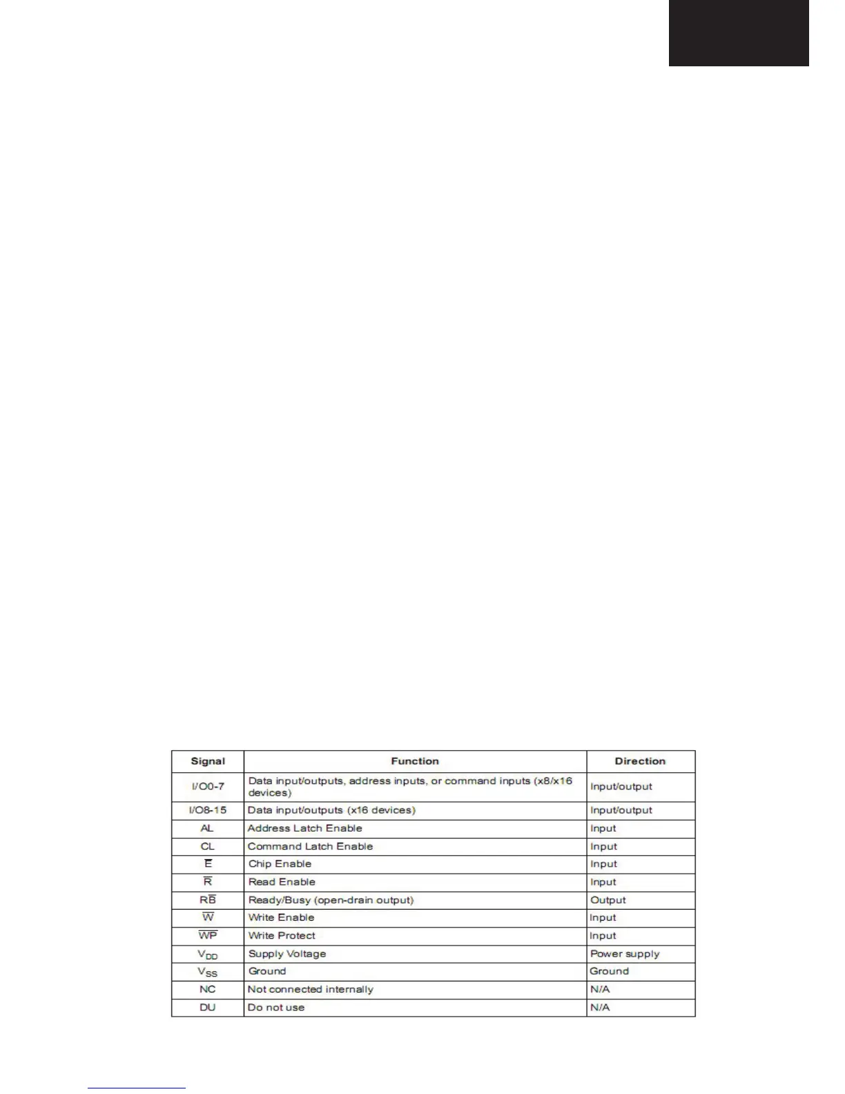
b) Pinning
49
LC-32LE340/343
LC-40LE340/343