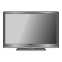
LC-32LE340/343
LC-40LE340/343
27
9. 32M x 16 bit DDRII Synchronous DRAM (U28-U29)
EtronTech EM68B16CWPA
a) Key Features
• JEDEC Standard Compliant
• JEDEC standard 1.8V I/O (SSTL_18-compatible)
• Power supplies: VDD & VDDQ = +1.8V ± 0.1V
• Operating temperatue: 0 – 85 °C
• Supports JEDEC clock jitter specification
• Fully synchronous operation
• Fast clock rate: 333/400MHz
• Differential Clock, CK & CK#
• Bidirectional single/differential data strobe
-DQS & DQS#
• 4 internal banks for concurrent operation
• 4-bit prefetch architecture
• Internal pipeline architecture
• Precharge & active power down
• Programmable Mode & Extended Mode registers
• Posted CAS# additive latency (AL): 0, 1, 2, 3, 4, 5
• WRITE latency = READ latency - 1 tCK
• Burst lengths: 4 or 8
• Burst type: Sequential / Interleave
• DLL enable/disable
• Off-Chip Driver (OCD)
-Impedance Adjustment
-Adjustable data-output drive strength
• On-die termination (ODT)
• RoHS compliant
• Auto Refresh and Self Refresh
• 8192 refresh cycles / 64ms
• Package: 84-ball 10x12.5x1.2mm (max) FBGA
- Pb and Halogen Free
The EM68B16C is a high-speed CMOS Double-Data-Rate-Two (DDR2), synchronous
dynamic random-access memory (SDRAM) containing 512 Mbits in a 16-bit wide data I/Os.
It is internally configured as a quad bank DRAM, 4 banks x 8Mb addresses x 16 I/Os The
device is designed to comply with DDR2 DRAM key features such as posted CAS# with
additive latency, Write latency = Read latency -1, Off-Chip Driver (OCD) impedance
adjustment, and On Die Termination(ODT). All of the control and address inputs are
synchronized with a pair of externally supplied differential clocks. Inputs are latched at the
cross point of differential clocks (CK rising and CK# falling) All I/Os are synchronized with a
pair of bidirectional strobes (DQS and DQS#) in a source synchronous fashion. The address
bus is used to convey row, column, and bank address information in RAS #, CAS#
multiplexing style. Accesses begin with the registration of a Bank Activate command, and
then it is followed by a Read or Write command. Read and write accesses to the DDR2
SDRAM are 4 or 8-bit burst oriented; accesses start at a selected location and continue for a
programmed number of locations in a programmed sequence. Operating the four memory
banks in an interleaved fashion allows random access operation to occur at a higher rate than
is possible with standard DRAMs. An auto precharge function may be enabled to provide a
self-timed row precharge that is initiated at the end of the burst sequence. A sequential and
gapless data rate is possible depending on burst length, CAS# latency, and speed grade of the
device.
b) Pinning
9. 32M x 16bit DDRII Synchronous DRAM (U28-U29)
45
LC-32LE340/343
LC-40LE340/343
 Loading...
