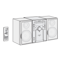
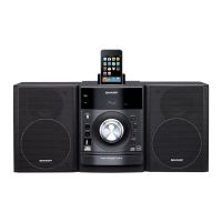
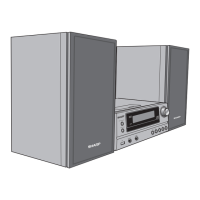
XL-DK257N
8 – 5
IC1 VHITC94A70FG2: CD MP3 DECODER (3/4)
Pin Description
Pin
No.
Symbol Input / Output Description Default Remarks
49 Pio1
Input / Output
3I/F
DSP general input/output port -1. Input Schmitt input CMOS PORT
50 Pio2
Input / Output
3I/F
DSP general input/output port -2. Input Schmitt input CMOS PORT
51 Pio3
Input / Output
3I/F
DSP general input/output port -3. Input Schmitt input CMOS PORT
52 VSS - Grounding pin for 3.3V digital circuit. - -
53 VDDT3 - Power supply pin for 3.3 V digital I/O circuit. - For CD and DSP I/O
54 SBSK Output 3AI/F Sub code block sync output pin. Output CMOS PORT
55 SBOK Output 3I/F CRCC check result output pin for sub code Q data. Output CMOS PORT
56 IPF Output 3I/F Correction flag output. Output CMOS PORT
57 SFSY Output 3I/F Servo internal register read clock output pin. Output CMOS PORT
58 ZDET Output 3I/F Internal Audio DAC Zero data detection flag output. Output CMOS PORT
59 GPIN Input 3I/F
CD General Input port (Pull down by 100KΩ when not
in use).
Input Schmitt input
60 MS Input 3I/F
Microprocessor I/F mode selection pin.
“H”: Parallel I/F, “L”: Serial I/F
Input
61 DoUT(Po6) Output 3I/F
Digital Audio output (SPDIF) pin
(DSP general output port -6)
Output CMOS PORT
62 AoUT1(Po7) Output 3I/F
Audio data output pin -1
(DSP general output port -7)
Output CMOS PORT
63 BCKo(Po8) Output 3I/F
Bit clock output pin for AoUT
(DSP general output port -8)
Output CMOS PORT
64 LRCKo(Po9) Output 3I/F
L/R channel clock output pin
(DSP general output port -9)
Output CMOS PORT
65 AiN(Pi4) Input 3I/F
Audio data input for Audio DAC
(DSP general input port -4)
Input Schmitt input
66 BCKi(Pi5) Input 3I/F
Bit clock input pin for AiN
(DSP general input port -5)
Input Schmitt input
67 LRCK(Pi6) Input 3I/F
L/R channel clock for AiN
(DSP general input port -6)
Input Schmitt input
68 VDD1 - Power supply pin for 1.5V digital circuit. -
69 VSS - Grounding pin for 1.5V digital circuit. -
70 AWRC Output 3AI/F VCO control pin for active wide-range PLL. Output
Applicable in CLV/CAV mode.
Connect 0.033 uF.
71 PVDD3 - Power supply pin for 3.3V CD PLL circuit. -
72 PDo Output 3AI/F EFM and PLCK Phase difference signal output pin. Output
4-state output ( PVDD3,
Hiz,PVSS3,PVREF)
73 TMAXS Output 3AI/F TMAX detection result output pin. Output
3-state output
(PVDD3,PVSS3,HiZ)
74 TMAX Output 3AI/F TMAX detection result output pin. Output
3-state
output(PVDD3,PVSS3,HiZ)
75 LPFN Input 3AI/F PLL circuit LPF amplifier inversion input pin. Input
Connect resister of LPF, refer
to application circuit diagram.
76 LPFo Output 3AI/F PLL circuit LPF amplifier Output pin. Output
Connect capacitor of LPF, refer
to application circuit diagram.
77 PVREF - PLL circuit 1.65 V reference voltage pin. -
Connected to VREF and VRO
inside of IC. Connect 0.1uF.
78 VCoF Output 3AI/F VCO filter pin Output Connect 0.01uF.
79 PVSS3 - Grounding pin for 3.3V CD PLL circuit. -
80 SLCo Output 3AI/F
EFM slice level output pin.
Output impedance =2.5kΩ both of
analog/digital slice mode.
Output
Connect capacitor according
with servo frequency band.
81 RFi Input 3AI/F
RF signal input pin
Zin is selectable by command.
Input Zin: 20kΩ, 10kΩ, 5kΩ
82 RFRPi Input 3AI/F RF ripple signal input pin. Input -
83 RFEQo Output 3AI/F RF equalizer circuit output pin. Output
Connect to RFRPI by 0.1uF, to
RFI by 4700pF.
84 Vro Output 3AI/F 1.65 V reference voltage output pin. Output
Connected to VREF and
PVREF inside of IC.
Connect 0.1uF+100uF.
85 RESiN Output 3AI/F
Pin for connecting a resistor for reference current
generation.
Output Connect 22k//0.01uF.
86 VMDiR Reference voltage output pin for LD APC. Connect 0.1uF.
87 TESTR Output 3AI/F
LPF connection pin for RFEQO offset correction
circuit.
Output Connect more than 0.015uF.