User Manual of A90 Series Inverter
212
The response delay (t
wait2
) is defined as the time interval from the reception of the
valid data frame 1 by the inverter to data parsing and return. To ensure the stable operation
of the protocol chip, the response delay should be set within 1-20ms (it must not be set to 0).
If the communication data involves EEPROM operation, the actual response delay
time will be extended, i.e. “EEPROM operation time + F10.04”.
1: valid data frame: sent by the external master station to inverter, in which the function
code, data length and CRC are correct.
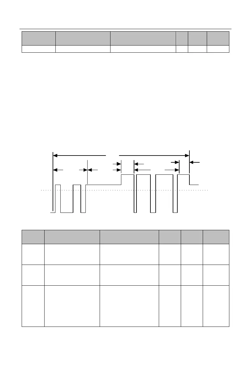
Fig. 7-30 shows the data sending segment (t
send
), sending end segment (t
wait1
),
75176-to-sending wait segment (t
wait2
), data return segment (t
return
), and 75176-to-receiving
wait segment (t
wait3
).
tsend twait 1
twait 2
treturn
twait 3
t
Fig. 7-30 Parsing Diagram of Complete Data Frame Timing
Options of master-slave
communication
function
0: slave
1: host (Modbus protocol
broadcast transmission)
0: output frequency
1: set frequency
2: output torque
3: set torque
4: PID setting
5: output current
 Loading...