3-4. Bl BOARD
3-4-1. Red Screen SW,AGC Pulse Insertion
(Same as Green and Blue)
Red signal can be cut off by RED SCREEN SW on the front panel.
Horizontal rate AGC pulse is removed and the reference pulse is
inserted in the signal for the GAIN and BIAS adjustment of video
output amplifier and for the beam control circuit.
3-4-2. Red Limitter, Gain Bias Control Amplifier
This limitter is used for limiting the excess input level of the signal
below 0V DC.
The GAIN/BIAS CONTROL amplifier is composed of variable
resistor element and transistors as same as contrast control am-
plifier' (See section of BH board)
3-4-3. Red Feedback Amplifier, Red Gain Control
Red Bias Control Circuit
RED FEEDBACK amplifier inverts the phase of the signal derived
from VIDEO OUTPUT amplifier via NF BUFF (Negative Feedback
Buffer) in BK board.
The BIAS of VIDEO OUTPUT AMPLIFIER is controlled by RED
BIAS CONTROL circuit so that the black level of inverted signal
may be OV DC.
(This time, black level of VIDEO OUTPUT will be -90V DC.)
RED GAIN CONTROL circuit controls the gain of VIDEO OUT-
PUT AMPLIFIER so that the level of the reference pulse may
match to the voltage at pin G) of 1C-t03.
(When GAIN control (RED) in the drawer is turned, the level of
the reference pulse inserted in section I changes. And amplitude
(Gain) of Red signal changes so that the amplitude of the reference
pulse derived from RED FEEDBACK amplifier may be maintained
constant by GAIN CONTROL circuit.)
3-4-4. Red Cathode Current Detection, Red G1 Control
Circuit 0-V Conversion)
Refer to the BK board section of beam control circuit
3-4-5. ABL Detector, Drive Control, Over Drive
The reference level of GAIN CONTROL circuit is controlled by
ABL detector and DRIVE CONTROL so that the cathode current
of CRT exceeds the predetermined (Preset) value to prevent damage
of CRT OVER DRIVE circuit lights up the OVER LOAD LED
on the front panel for warning.
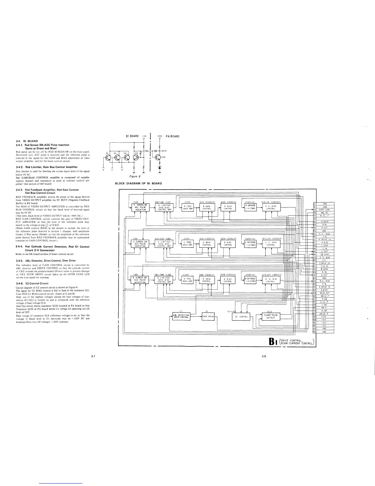
3-4-6. G2 Control Circuit
Circuit diagram of G2 control circuit is shown in Figure 6.
The signal for Gl BIAS control is fed to base of the transistor QI I
from RED GI BIAS control circuit. (Same as G and B)
Only one of the highest voltages among the base voltages of tran-
sistors QI l ·Ql 3 is turned on and is compared with the reference
voltage of base voltage Ql4.
And this circuit drives transistor Ql05 located in PA board so that
Transistor Ql05 in PA board drives G2 voltage for adjusting cut off
level of CRT.
Base voltage of transistor Ql4 (reference voltage) is set so that the
voltage of Black level at G 1 electrode may be - l 20V DC and
maintain Ekco (cut off voltage) -l 20V constant.
3-7
8 I BOARD +I2v
+
4
iov p A 8 OARD
G2
Figure 6
BLOCK DIAGRAM OF Bl BOARD
- ------------------
------------------------------------,
iCIOI
0I0I~Ios ,cI02
ICl04 0110 ICI03(1/21
1
R SCREEN SW
R LIMITTER
~
y R FEED ~M
AGC PULSE
GAIN,81AS
R GAIN
INSERTION
CONTROL AMP
BACK AMP
CONTROL
i
l t
I
I
0109 ICl03(2/21
R BIAS
CONTROL
~
ICI051I/21
R CATHODE
1-V CONV
0113, 114 ICl0512/2 I
R GI BIAS I
1-----~
CONTROL I
f 1
Al
81
~
A2
-
B2
3
83
A4
B4
.-----+===========,--=_=_ =_ =_ =_ =_ =_ =_ =_ =_ =_ =_ =_ =_ =_ =_ ==_ ==_ ==_ =_ =_ =_ =_ =_ =_ =_ =_ =_ =_ ±tt±±±:1:-h 1m--i--
A5
85
"6
B6
ICZOI
0201-208 IC202
1(204 0210 IC2031 l/21
0209 IC20312/2l IC205(1/21
0213,214 IC20512/21
y
G SCREEN SW
G LIMITTER
~
1
G FEED ~rl
G GAIN
I
M
8 BIAS
YG CATHODE
G GI BIAS
I
AGC PULSE
GAIN. Bl AS
INSERTION
CONTRCL AMP
BACK AMP
CONTROL CONTROL
1-VCONV
CONTROL
I
A7
87
AB
r
i
I t
r
r
L
I
BB
A9
,..
89
AIO
810
All
~,__
811
Al2
812
1(301
0301 ~308 ,uoz
IC304 0310 IC303W21 0309 IC30312/21
Al3
813
GND
GND
OVER LOAD
ABL. IN
B. CL. P
R.GAIN
R.IN
R.OUT
GND
R.
CL. BIAS
K. R
R.DRIVE.IN
R. BIAS
G. GAIN
G. IN
G. OUT
G2. CONT
G. CL. BIAS
K.G
G.DRIVE. IN
G. 8. AS
8.GAIN
8. IN
B. OUT
GND
Y
8 SCREEN SW
AGC PULSE
INSERTION
8 LIMITTER
~
GAIN.BIAS
CONTROL AMP
Y B~c:E!~P
~
ri cBoN~~~~ I rl ~oN
8
T
1
RAOSL
I C3051I/21
I _Is CATHODE
1
1-VCONV
0313, 314 1(30512/21
B GI Bl AS l
CONTRCL 1rc.+!-+-!-+-!-+-!-+-t-----Hf-+--..J,__+---
Al4 B.CL.8IAS
LJ 1
: I i L
L,_ _____________ ':_-...j+_-_-_-_-_-_-_J-+--t-L.- -_ -_ -_ -_ -_ -_ -_ -_ -_ -_ -_ -_ -_ -_ -_ -_ -_ -_ -_ -_ -_ --<_'"_ -_ -_ -_ -_ -_ -_ -_ -_ -_ -_ -l .... ~J-le-i-l-l-l-4~..J..J. ,......,.+---+++..-!
I
814
Al5
815
IC I
QI
_JABL DETECTION I-- I l
1
DRIVE CONTROL
1
i-----
1
ovrn DRIVEr
- ----------------
AIE
816
Al7
817
01h15 l 02 3
,......-~-~........,
I
L
~
CLAMP PULSE I
G2 coNrno L I [ I i.___D_E_T_E_c_r_ ............ -----'
Al8
818
Al9
19
Az<.
Bz<.
A21
£21
A2
82,
B
I
(
DRIVE CONTROL, )
BEAM CURRENT CONTROL
----------'
3-8
K.B
8.DRIVE. IN
B.BIAS
BLUE .OUT
BM.CL. P
R.SW
D .CL.P
G. SW
BM.P
B.SW
DRIVE. P
+ 12V
+12V
-I2V
-I2V
GNO
GNO