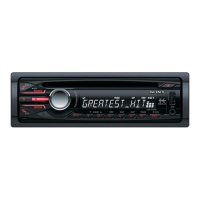
CDX-GT50UMS/GT450U/GT457UE/GT500U/GT500US/GT505U
26
• IC Pin Function Description
MAIN BOARD (2/3) IC501 R5F3650KBDZ99FA (SYSTEM CONTROL)
Pin No. Pin Name I/O Description
1 LCD_SO O Serial data output for LCD driver
2 LCD_CLK O Serial clock signal output for LCD driver
3
NOSE_SW I Front panel detach detect signal input (Fixed at L in this set)
4 SIRCS I SIRCS signal input
5 UNISO O SONY BUS serial data output (Not used in this set)
6 UNISI I SONY BUS serial data input (Fixed at L in this set)
7 UNISCK O SONY BUS serial clock signal output (Fixed at L in this set)
8 BYTE I External data bus width select signal input (Connect to VSS in this set)
9 CNVSS I Flash writer IF (CNVSS) signal input (L: normally operation, H: fl ash write)
10 XIN I Low speed operation clock signal input (32.768 kHz)
11 XOUT O Low speed operation clock signal output (32.768 kHz)
12
RESET I System reset signal input
13 OSCOUT O High speed operation clock signal output (7.92 MHz)
14 VSS — Ground
15 OSCIN I High speed operation clock signal input (7.92 MHz)
16 VCC1 — Power supply pin (+3.3 V)
17
NMI I Non-maskable interrupt signal input (Fixed at H in this set)
18
RC_IN1 I Rotary commander shift key signal input
19 BUIN I Backup power supply detect signal input
20
SYSRST O System reset signal output
21
BUS_ON O VBUS power control signal output (Not used in this set)
22 MC_RX I MC-BUS communication MECHA (CMX-101Z) TX signal input
23 NCO O Not used. (Open)
24 MC_TX O MC-BUS communication MECHA (CMX-101Z) RX signal output
25 NCO O Not used. (Open)
26 SYNC_OUT O DD converter frequency control signal output
27 NCO O Not used. (Open)
28 BEEP O Beep signal output for the power amplifi er IC
29 I2C_SCK O IIC communication serial clock signal output
30 I2C_SIO I/O IIC communication serial data input/output
31 FW_TXD O Flash writer IF (serial data) output
32 FW_RXD I Flash writer IF (serial data) input
33 FW_CLK I Flash writer IF (serial clock) signal input
34 FW_BUSY O Flash writer IF (busy) signal output
35, 36 NCO O Not used. (Open)
37 CD_ON I CD mechanism servo power supply control request signal input
38 CDM_ON I CD mechanism deck power supply control request signal input
39 WAKE_UP O CD mechanism deck micon wake up signal output
40 Z_MUTE I Z mute signal input
41 EPM O EPM signal output (Fixed at L in this set)
42 MODELNAME_SEL0 I Model name select signal input 0 (Fixed at L in this set)
43 MODELNAME_SEL1 I Model name select signal input 1 (Fixed at L in this set)
44 MODELNAME_SEL2 I Model name select signal input 2 (Fixed at L in this set)
45 MODELNAME_SEL3 I Model name select signal input 3 (Fixed at L in this set)
46 CE O CE signal output (Fixed at H in this set)
47 NCO O Not used. (Open)
48 SA_DATAIN I Paradisso spectrum analyzer serial data input
49 SA_CLKOUT O Paradisso spectrum analyzer serial clock signal output
50 USBON O USB over current detect IC control signal output
51 VBUS_ON I VBUS power supply control signal input (L: VBUS OFF, H: VBUS ON)
52
USB_OVR I USB over current detect signal input
53
EXTATT_XEN O
L is sent when electronic volume IC has the status of CD/USB (H is sent when it has the
status of other source) (Not used in this set)
54, 55 NCO O Not used. (Open)
56 TELATT I Telephone attenuator detect signal input (AEP, UK, Russian model)
57
ACC_IN I Accessory power supply detect signal input
58 ATT O Audio mute control signal output
 Loading...