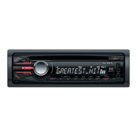
CDX-GT50UMS/GT450U/GT457UE/GT500U/GT500US/GT505U
27
Pin No. Pin Name I/O Description
59 DIAG I Condition signal input from power amp IC
60 AMPSTB O Standby signal output for power regulator IC
61 CYRIL_SEL I
Cyril correspondance discrimination signal input (L: No correspondance) (Fixed at L in this
set)
62 VCC2 — Power supply pin (+3.3 V)
63 NCO O Not used. (Open)
64 VSS — Ground
65 ILLUMI SEL I Key illumination voltage setting signal input
66 COLSW SEL I Key illumination color change function signal input
67 NCO O Not used. (Open)
68 B-OUT SEL I Black out function setting signal input (L: without black out function)
69 AREASEL3 I Destination setting pin 3 (Fixed at L in this set)
70 AREASEL2 I Destination setting pin 2
71 AREASEL1 I Destination setting pin 1
72 AREASEL0 I Destination setting pin 0
73 R/S SW SEL I REAR/SUB select setting signal input (L: No switched) (Fixed at H in this set)
74, 75 NCO O Not used. (Open)
76 INITCOL_SEL I Key illumination initial color setting signal input
77, 78 NCO O Not used. (Open)
79, 80 DEBUG_1, DEBUG_2 O Not used. (Open)
81
RE-IN1 I Rotary encoder signal input 1
82
RE-IN0 I Rotary encoder signal input 0
83 to 90 NCO O Not used. (Open)
91
KEYACK0 I Key acknowledge detect signal input (Rotary commander)
92
KEYACK1 I Key acknowledge detect signal input (Front panel)
93 NCO O Not used. (Open)
94 KEYIN1 I Key signal input 1
95 KEYIN0 I Key signal input 0
96 AVSS — Ground for A/D converter
97 RC_IN0 I Rotary commander key signal input
98 AVRH — A/D converter external reference power supply pin (+3.3 V)
99 AVDD — A/D converter power supply pin (+3.3 V)
100 LCD_CE O Chip enable signal output for LCD driver
 Loading...