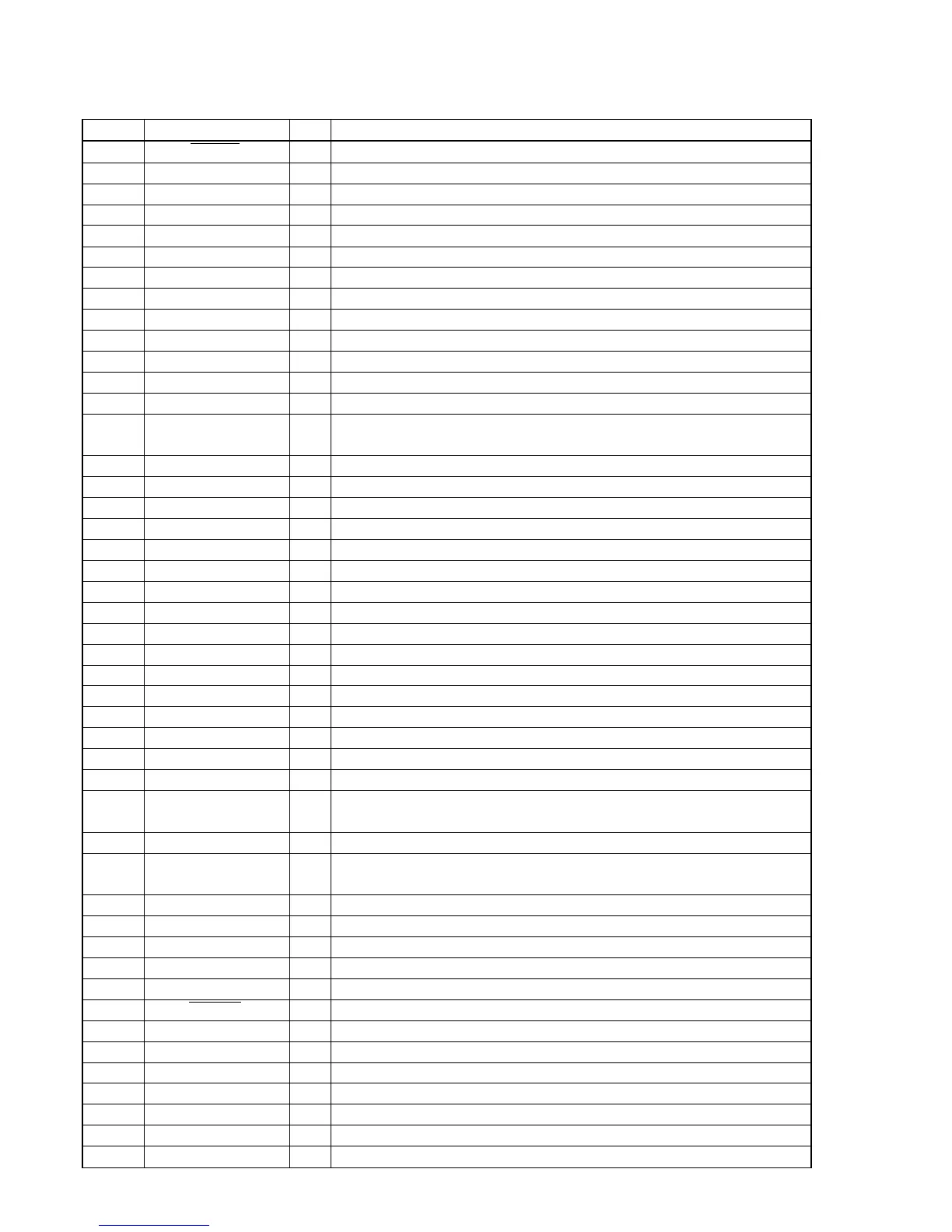
44
CDX-GT71W/GT710/GT760
IC901 M30876FJBA01GP (DISPLAY CONTROL) (DISPLAY BOARD)
Pin No. Pin Name I/O Pin Description
1 SYS CE I Main chip enable signal input
2NCONot used in this set. (Open)
3FL DAT3 O Vacuum fluorescent displays serial data signal output 3
4NCONot used in this set. (Open)
5 FL CLK IN I Vacuum fluorescent displays serial clock signal input
6 BYTE I Connect to ground. (Fixed to “L”.)
7 CNVSS I Port for flash write H (write switch) Normally operation: “L”
8, 9 NC O Not used in this set. (Open)
10 RESET I Reset signal input
11 XOUT O Main clock signal output (6.75 MHz)
12 VSS — Ground pin
13 XIN I Main clock signal input (6.75 MHz)
14 VCC1 — Power supply pin (+3.3 V)
15 NMI I
Non-maskable interruption signal input
Fixed to “H” for external pull-up resistor.
16 to 18 NC O Not used in this set. (Open)
19 GCP TA4 IN I Vacuum fluorescent displays GCP TA4 signal input
20, 21 NC O Not used in this set. (Open)
22 BK TA3 OUT O Vacuum fluorescent displays BK TA3 signal output
23 NC O Not used in this set. (Open)
24 LAT TA2 OUT O Vacuum fluorescent displays latch TA2 signal output
25 to 27 NC O Not used in this set. (Open)
28 GCP TA0 OUT O Vacuum fluorescent displays GCP TA0 signal output
29 SYS SO O Main serial data signal output
30 SYS SI I Main serial data signal input
31 SYS CLK I Main serial clock signal input
32 NC O Not used in this set. (Open)
33 FL DAT1 O Vacuum fluorescent displays serial data signal output 1
34 NC O Not used in this set. (Open)
35 FL CLK I Vacuum fluorescent displays serial clock signal input
36 to 38 NC O Not used in this set. (Open)
39 HOLD I
External data bus (Hold) signal input
Fixed to “L” for external pull-down resistor.
40 to 43 NC O Not used in this set. (Open)
44 WRI/WR I
External data bus (WRI/WR) signal input
Fixed to “H” for external pull-up resistor.
45 to 59 NC O Not used in this set. (Open)
60 VCC2 — Power supply pin (+3.3 V)
61 NC O Not used in this set. (Open)
62 VSS — Ground pin
63 to 70 NC O Not used in this set. (Open)
71 PLUG IN I AUX plug detect signal input
72 to 84 NC O Not used in this set. (Open)
85 KEY 1 I Key signal input 1
86 KEY 2 I Key signal input 2
87, 88 NC O Not used in this set. (Open)
89 SIRCS I SIRCS data signal input
90 NC O Not used in this set. (Open)
91 ILL BLUE O Illumination (blue) change control signal output
 Loading...