10
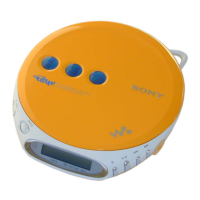
D-EJ750/EJ751/EJ753/EJ755/EJ756CK/EJ758CK
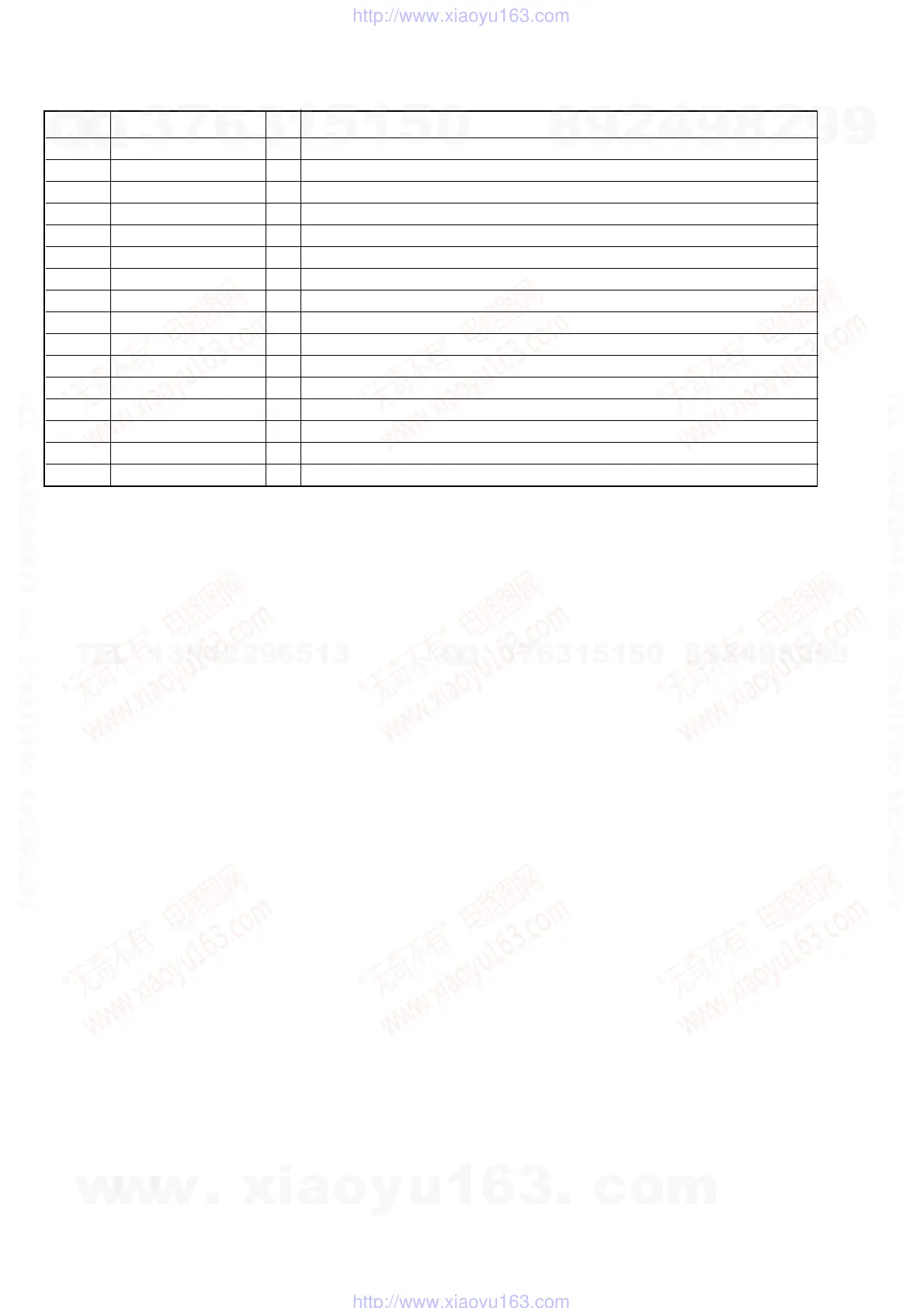
Pin No. Pin name I/O Description
105 VDD2 – Power supply terminal for digital.
106 LRCK O LR clock output for D/A interface.
107 LRCKI I LR clock input for D/A interface.
108 PCMD O Serial data output for D/A interface.
109 PCMDI I Serial data input for D/A interface.
110 BCK O Bit clock output for D/A interface.
111 BCKI I Bit clock intput for D/A interface.
112 DVDD – Power supply for DRAM interface.
113 A3 O DRAM adress 3.
114 A2 O DRAM adress 2.
115 A1 O DRAM adress 1.
116 A0 O DRAM adress 0.
117 A10 O DRAM adress 10.
118 A11 I/O Not used (OPEN).
119 TEST3 O Not used (OPEN).
120 TEST4 O Not used (OPEN).
w
w
w
.
x
i
a
o
y
u
1
6
3
.
c
o
m
Q
Q
3
7
6
3
1
5
1
5
0
9
9
2
8
9
4
2
9
8
T
E
L
1
3
9
4
2
2
9
6
5
1
3
9
9
2
8
9
4
2
9
8
0
5
1
5
1
3
6
7
3
Q
Q
TEL 13942296513 QQ 376315150 892498299
TEL 13942296513 QQ 376315150 892498299
http://www.xiaoyu163.com
http://www.xiaoyu163.com