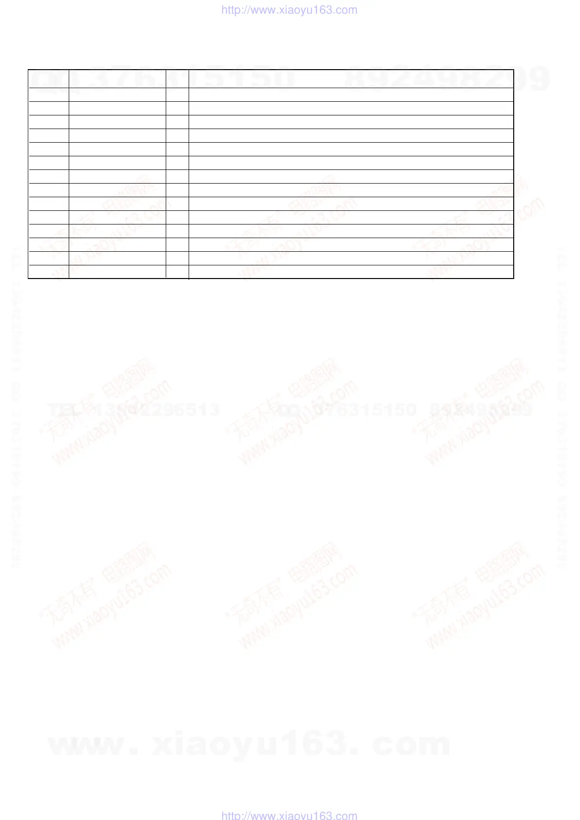
12
D-EJ750/EJ751/EJ753/EJ755/EJ756CK/EJ758CK
Pin No. Pin name I/O Description
67 SO_O O Serial data clock output.
68 PGMSI_I I Serial date input.
69 PGMSCK_O O Serial data output.
70 AGCPWM_O O PWM output for laser AGC.
71 IR_RMC_I I Not used (Fixed to “H”).
72 FG_I/FGSEL_I I FG input / spindle motor select.
73 PGMSEL_O O EEPROM write control.
74 XDRVLT_O O Not used (OPEN).
75 XPOWLT_O O Data latch output for power IC.
76 XRST_O O System reset output.
77 HG_XSTB_O O HG sleep mode output.
78 HG_GUP_O O HG gain up output.
79 NC – Not used (OPEN).
80 NJR_I I Not used (Fixed to “H”).
w
w
w
.
x
i
a
o
y
u
1
6
3
.
c
o
m
Q
Q
3
7
6
3
1
5
1
5
0
9
9
2
8
9
4
2
9
8
T
E
L
1
3
9
4
2
2
9
6
5
1
3
9
9
2
8
9
4
2
9
8
0
5
1
5
1
3
6
7
3
Q
Q
TEL 13942296513 QQ 376315150 892498299
TEL 13942296513 QQ 376315150 892498299
http://www.xiaoyu163.com
http://www.xiaoyu163.com