5.7 µs
Note on Printed Wiring Board
• X : parts extracted from the component side.
• Y : parts extracted from the conductor side.
• : Pattern from the side which enables seeing.
(The other layers' patterns are not indicated.)
•Abbreviation
FR : French model
Caution:
Pattern face side: Parts on the pattern face side seen from
(Conductor Side) the pattern face are indicated.
Parts face side: Parts on the parts face side seen from
(Component Side) the parts face are indicated.
Note on Schematic Diagram:
• All capacitors are in µF unless otherwise noted. pF: µµF
50 WV or less are not indicated except for electrolytics
and tantalums.
• All resistors are in Ω and
1
/
4
W or less unless otherwise
specified.
•%: indicates tolerance.
• C : panel designation.
• A : B+ Line.
•Total current is measured with CD installed.
•Power voltage is dc 4.5 V and fed with regulated dc power
supply from DC IN 4.5V jack (J401).
•Voltages and waveforms are dc with respect to ground in
CD play mode.
no mark : CD PLAY
•Voltages are taken with a VOM (Input impedance 10 MΩ).
Voltage variations may be noted due to normal produc-
tion tolerances.
•Waveforms are taken with a oscilloscope.
Voltage variations may be noted due to normal produc-
tion tolerances.
• Circled numbers refer to waveforms.
• Signal path.
J : CD PLAY
•Abbreviation
FR : French model
5-3. NOTE FOR PRINTED WIRING BOARDS AND SCHEMATIC DIAGRAMS
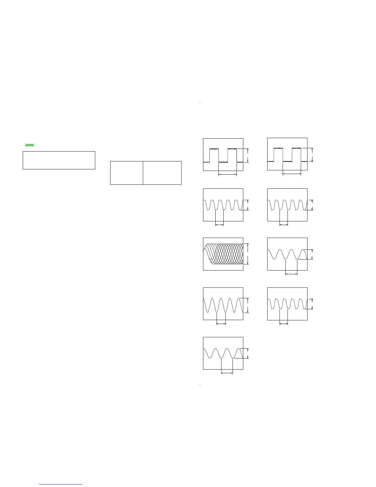
3 IC601 qd (RFI)
4 IC601 ek (XOUT)
5 IC601 td (CLK4M)
6 IC601 ua (CLKDRV)
7 IC401 wh (CLOCK)
8 IC801 2 (XIN)
1 Vp-p
236 ns
1 Vp-p
236 ns
•Waveforms
1 IC406 1 (SYNC)
9 IC801 qk (SCK)
84 Vp-p
20 ms
Note:
The components identi-
fied by mark 0 or dotted
line with mark 0 are criti-
cal for safety.
Replace only with part
number specified.
Note:
Les composants identifiés par
une marque 0 sont critiques
pour la sécurité.
Ne les remplacer que par une
pièce portant le numéro
spécifié.