4
DP-RF6000
SECTION 2
DIAGRAMS
For schematic diagrams.
Note:
• All capacitors are in µF unless otherwise noted. (p: pF) 50 WV or
less are not indicated except for electrolytics and tantalums.
• All resistors are in Ω and
1
/
4
W or less unless otherwise specified.
•%: indicates tolerance.
• f : internal component.
• C : panel designation.
• A : B+ Line.
• Power voltage is dc 9 V and fed with regulated dc power supply
from external power voltage jack.
•Voltages and waveforms are dc with respect to ground under no-
signal conditions.
•Voltages are taken with a VOM (Input impedance 10 MΩ).
Voltage variations may be noted due to normal production toler-
ances.
•Waveforms are taken with a oscilloscope.
Voltage variations may be noted due to normal production toler-
ances.
• Circled numbers refer to waveforms.
• Signal path.
F : ANALOG
J : DIGITAL
NOTE FOR PRINTED WIRING BOARDS AND SCHEMATIC DIAGRAMS.
For printed wiring boards.
Note:
• X : parts extracted from the component side.
• f : internal component.
• : Pattern from the side which enables seeing.
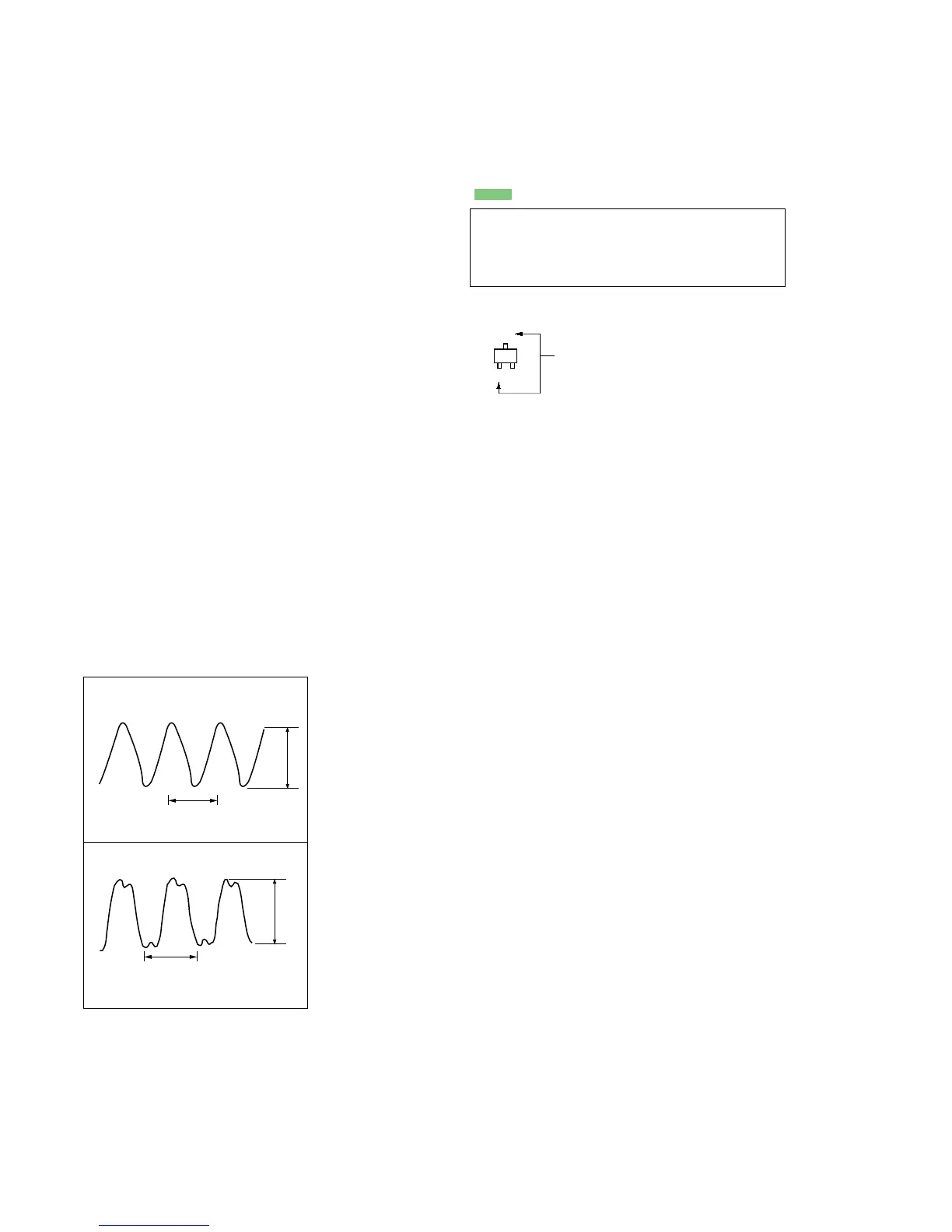
• Waveforms
– TX BOARD –
C
B
These are omitted.
E
Q
0.5V/DIV, 0.1
µ
sec/DIV
1
IC201
XO
i;
1.5Vp-p
1V/DIV, 20 nsec/DIV
2
IC4001 A
2
3.8Vp-p
203 ns
83.2 ns
• Indication of transistor.
Caution:
Pattern face side: Parts on the pattern face side seen from
(Side B) the pattern face are indicated.
Parts face side: Parts on the parts face side seen from
(Side A) the parts face are indicated.