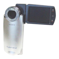
EasyManua.ls Logo

Sony DSC-M1 - Page 35

Sony DSC-M1
54 pages
Print Icon
To Next Page IconTo Next Page
To Previous Page IconTo Previous Page
Loading...
DSC-M1
4-47
4-3. PRINTED WIRING BOARDS
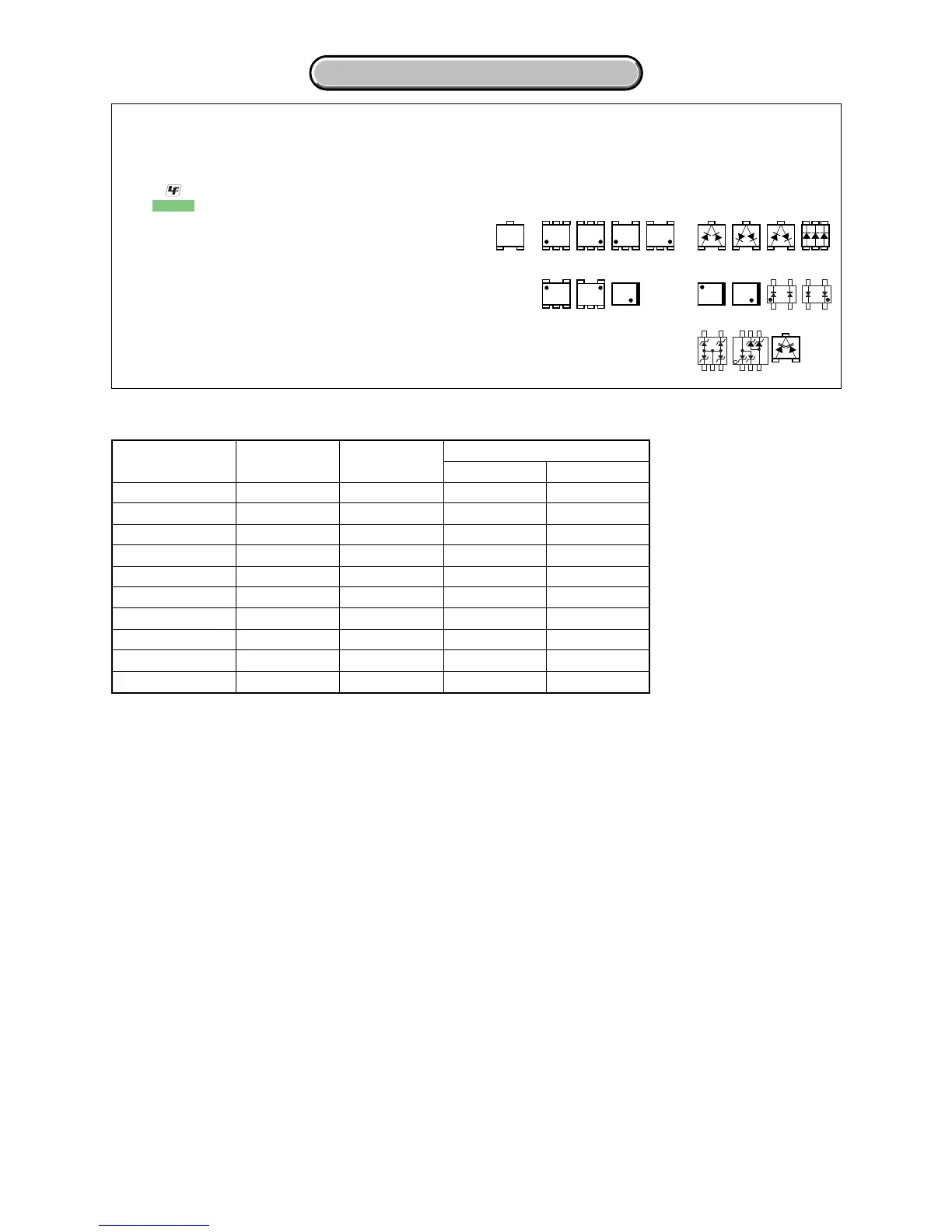
(For printed wiring boards)
: Uses unleaded solder.
: Pattern from the side which enables seeing.
(The other layers patterns are not indicated)
Through hole is omitted.
Circled numbers refer to waveforms.
There are a few cases that the part printed on diagram
isnt mounted in this model.
C: panel designation
THIS NOTE IS COMMON FOR WIRING BOARDS
(In addition to this, the necessary note is printed in each block)
Chip parts.
Transistor Diode
21
3
12
3
21
3
21
3
345
21
123
654
EB
C
31
5
5
2
46
123
54
43
12
5
4
1
3
12
43
312
45
534
12
34
21
12
43
46
2
5
31
12
4
3
64
1
3
board name
FP-035
FP-036
FP-037
FP-038
FP-040
FP-041
LD-175
MS-252
PM-045
SY-114
parts location
(shown on page)
4-63
4-63
4-64
number of layers
1
2
2
1
1
1
4
2
4
8
layers not shown
2 to 3
2 to 3
2 to 7
pattern
BOARD INFORMATION
waveforms
(shown on page)
4-61
4-62

Related product manuals