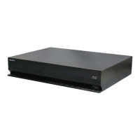
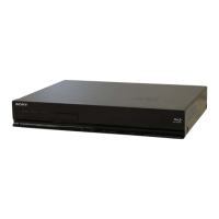
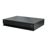
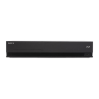
HBD-E370/E470/E570/E870/T57
89
MAIN BOARD IC501 R5F364AMDFA (SYSTEM CONTROLLER)
Pin No. Pin Name I/O Description
1 DAMP_SCDT/DIR_DI O Serial data output to the stream processor
2
DAMP_SHIFT/
DIR_CL
O Serial data transfer clock signal output to the stream processor
3 FL_CS O Chip select signal output to the fl uorescent indicator tube driver
4 SIRCS_IN I SIRCS signal input from the remote control receiver
5 FL_DOUT O Serial data output to the fl uorescent indicator tube driver
6 CEC_RX_IN - Not used
7 FL_CLK O Serial data transfer clock signal output to the fl uorescent indicator tube driver
8 BYTE I External data bus width selection signal input terminal
9 CNVss I Processor mode selection signal input terminal
10 Xcin I Sub system clock input terminal Not used
11 Xcout O Sub system clock output terminal Not used
12 RESET I System reset signal input from the reset signal generator
13 Xout O Main system clock output terminal (6 MHz)
14 Vss - Ground terminal
15 Xin I Main system clock input terminal (6 MHz)
16 Vcc - Power supply terminal (+3.3V)
17 CEC (TX/RX) I/O CEC serial data input/output with the HDMI ARC OUT connector
18 NO USE - Not used
19 KEY_INT I Key wake-up signal input terminal
20 AC_CUT I AC cut detection signal input terminal
21 BD_IF_START O Busy request signal output to the BD decoder
22 ST_DO I Serial data input from the tuner (FM)
23 ST_CLK O Serial data transfer clock signal output to the tuner (FM)
24 ST_DI O Serial data output to the tuner (FM)
25 BD_IF_REQ I Request signal input from the BD decoder
26 CEC_TX_OUT - Not used
27 PCONT_FL O Power on/off control signal output terminal for the front panel section
28 LED_PWM O LED drive signal output terminal
29 S-AIR_SDA I/O Two-way I2C data bus with the wireless transceiver
30 S-AIR_SCL O I2C clock signal output to the wireless transceiver
31 TXD1 - Not used
32 RXD1 - Not used
33 S-AIR_GPIO2 I Interrupt signal input from the wireless transceiver
34 S-AIR_ADC_SEL O Data selection signal output terminal for S-AIR section
35 BD_RESET O Reset signal output to the BD decoder, NAND fl ash, EEPROM and ethernet interface
36 BD_CS O Chip select signal output to the BD decoder
37 to 39
BD_PCONT1 to
BD_CONT3
O Power on/off control signal output terminal for the BD section
40 BD_PCONT4 O Power on/off control signal output terminal Not used
41, 42
BD_PCONT5,
BD_CONT6
O Power on/off control signal output terminal for the BD section
43 P_CONT1 O Power on/off control signal output terminal
44 FAN_ON O Power on/off control signal output terminal for the FAN motor
45 FAN_CONT O FAN motor on/off control signal output terminal
46 CE - Not used
47 BD_BDI O Serial data output to the BD decoder
48 BD_BDO I Serial data input from the BD decoder
49 BD_SCLK I Serial data transfer clock signal input from the BD decoder
50 DRIVER_RST (EN) O Reset signal output to the power amplifi er
51, 52
OVERFLOW1,
OVERFLOW2
O Overfl ow detection signal input from the stream processor
53 DAMP_INT O Reset signal output to the stream processor
54 DAMP_SOFT_MUTE O Soft muting on/off control signal output to stream processor
55 to 57
DAMP_LATCH1 to
DAMP_LATCH3
O Serial data latch pulse signal output to the stream processor
58 to 61 NO USE - Not used
62 Vcc - Power supply terminal (+3.3V)
63 S-AIR_SRC_RST O Reset signal output to the S-AIR section
64 Vss - Ground terminal