56
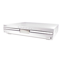
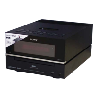
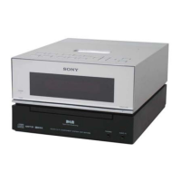
HCD-BC150/BC250
Ver 1.3
• MAIN BOARD IC509 uPD703261YGF-S21-JBT-A (SYSTEM CONTROLLER)
Pin No. Pin Name I/O Description
1 HP SW I Switch headphone is insert input
2 HP MUTE O Control of muting headphone signal output
3AVREF0 — Analog reference voltage for A/D converter
4AVSS — Analog ground
5V CONTROL O Voltage control signal output to the switching regulator
6AC_ON/OFF O AC power on/off signal output to the switching regulator
7AVREF1 — Analog reference voltage for D/A converter
8 DRIVE_OCP I Over load detect signal input
9 DRIVE_RST O System Reset signal output to the power driver
10 FLASH0 I Flash programing mode (pull down)
11 VDD — Power supply(+3.3V)
12 REGC — Regulator control-connect
13 VSS — Terminal Ground
14 X1 I Crystal input for main clock
15 X2 O Crystal output for main clock
16 RESET I System reset signal input
17 XT1 — Not used
18 XT2 — Not used
19 DIAT XRST — Not used
20 KEY INT I Wake up from ECO mode by key input
21 RM_INT I Wake up from ECO mode by sircs input
22 (Can’t USE) I Can’t Use Port
23 AC_CUT I Detect AC-CUT (primary power off)
24 NO USE — Not used
25 NO USE — Not used
26 NO USE — Not used
27 FL_D_OUT/LED_DATA O Data output to the FL driver/LED driver
28 NO USE — Not used
29 FL_CLK O Clock signal output to the FL driver/LED driver
30 FL_CS/STB O Chip select signal output to the FL driver
31 LED_RST O Reset signal output to the LED driver
32 BACK LIGHT O Back light output
33 STBY_LED O Standby LED control signal output
34 SIRCS_IN I Sircs input
35 EVSS — Terminal Ground
36 EVDD — Power supply(+3.3V)
37 12C DATA I/O
Two-way 12C data bus with the DVD system processor and mechanism controller
38 12C CLK I/O
Two-way 12C clock bus with the DVD system processor and mechanism controller
39 MUTE REQ O Mute Req signal output to the DSP
40 SYS RESET O Signal reset signal output to the DSP
41 LED LAT/DF INIT O LED LAT signal output to the LED driver
42 DIAT XSCEN — Not used
43
DIAT SDATA
O Digital amp serial data output
DAMP SCDT
44
DIAT SCLK/
O Digital amp shift clock signal data output
DAMP SHIFT
45 DAMP LATCH1 O Digital amp chip select1 signal output