Do you have a question about the Sony HCD-BC250 and is the answer not in the manual?
Details on power output and total harmonic distortion for amplifier sections.
Specifies input signal types and impedance characteristics.
Information on laser, signal format, and frequency response.
Details on tuner system, tuning range, antenna, and IF frequency.
Defines model abbreviations used throughout the manual.
Specifies AC leakage limits and testing methods for exposed metal parts.
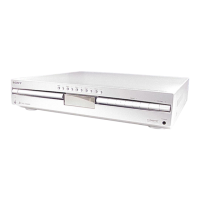
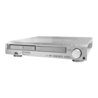
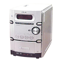
Identifies and describes controls and connectors on the front panel.
Identifies and describes connectors and terminals on the rear panel.
Shows the physical layout of components on the RF board.
Provides the circuit diagram for the RF section of the device.
Illustrates the component placement on the CD mechanism board.
Presents the circuit schematic for the CD mechanism section.
Shows component layout on the DMB07 board, side A.
Shows component layout on the DMB07 board, side B.
Part 1 of the schematic diagram for the DMB07 section.
Part 2 of the schematic diagram for the DMB07 section.
Part 3 of the schematic diagram for the DMB07 section.
Part 4 of the schematic diagram for the DMB07 section.
Part 5 of the schematic diagram for the DMB07 section.
Part 6 of the schematic diagram for the DMB07 section.
Part 7 of the schematic diagram for the DMB07 section.
Part 8 of the schematic diagram for the DMB07 section.
Shows component layout on the MAIN board, side A.
Shows component layout on the MAIN board, side B.
Part 1 of the schematic diagram for the MAIN section.
Part 2 of the schematic diagram for the MAIN section.
Shows component layout for panel, FL, power switch, and H/P/amp retainer boards.
Circuit schematic for panel, FL, power switch, and H/P/amp retainer boards.
Shows component layout on the IO board.
Circuit schematic for the IO section.
Shows component layout on the AMP board, side A.
Shows component layout on the AMP board, side B.
Part 1 of the schematic diagram for the AMP section.
Part 2 of the schematic diagram for the AMP section.
Part 3 of the schematic diagram for the AMP section.
Part 4 of the schematic diagram for the AMP section.
Shows component layout for SPK and LF boards.
Circuit schematic for the SPK and LF sections.
Illustrates the physical placement of various circuit boards within the unit.
Defines abbreviations used for components and models.
Shows specific waveforms related to the RF section's operation.
Displays waveforms from the DMB07 board for analysis.
Presents waveforms from the main board for analysis.
Displays waveforms associated with the IO board.
Shows waveforms from the amplifier section for diagnostic purposes.
Block diagrams for ICs within the RF section.
IC block diagrams for the translation board.
IC block diagrams for the panel board.
IC block diagrams for the FL board.
IC block diagrams for the DMB07 board, including detailed pinouts.
IC block diagrams for the main board, illustrating IC functions.
IC block diagrams for the IO board, showing functional blocks.
IC block diagrams for the amplifier section, detailing ICs like CXD9788AR.
Lists pin names, I/O, and descriptions for the DVD system processor IC.
Lists pin names, I/O, and descriptions for the RF amplifier IC.
Lists pin functions for the DVD decoder IC on the DMB07 board.
Details pin functions for the mechanism controller IC on the DMB07 board.
Lists pin functions for the system controller IC on the MAIN board.
Details pin functions for the power driver ICs on the AMP board.
Details pin functions for the DVD system processor IC on the DMB09 board.
Lists pin functions for the digital audio processor IC on the MAIN board.
Defines abbreviations for model names used in exploded views.
Shows the overall exploded view of the main chassis and front panel assembly.
Parts list specifically for the amplifier section components.
Checks system parameters like version, EEPROM, and GPIO.
Measures and writes the mirror time of a loaded disc to the EEPROM.
Measures and displays the error rate for PI and PO signals.
Initializes servo data and adjusts for DVD-SL, CD, and DVD-DL discs.
Detailed steps for adjusting a single-layer DVD disc.
Allows setting or checking the inserted disc type (DVD, CD, Hybrid).
Automatically judges the inserted disc type.
Allows manual selection of the disc type (DVD, CD, Hybrid).
Displays servo and mechanism error history information.
Illustrates the service position for the DVD mechanism deck.
Explains the disc tray lock function and its setting/releasing procedures.
Instructions for replacing the DMB07 board and initializing memory.
Procedure for disassembling the case and front panel assembly.
Procedure for disassembling the panel, FL, H/P, and power switch boards.
Procedure for disassembling the switching regulator.
Procedure for disassembling the amplifier board.
Procedure for disassembling the DMB07 board.
Procedure for disassembling the speaker, IO, and DC fan.
Procedure for disassembling the main board.
Procedure for disassembling the LF board.
Procedure for disassembling the MD rear cover.
Procedure for removing the DVD mechanism deck.
Procedure for disassembling the tray assembly.
Procedure for disassembling the motor boards and motors.
Procedure for disassembling the base unit.
Procedure for disassembling the RF board.
Procedure for disassembling the optical pick-up.
Explains the disc tray lock function and its setting/releasing procedures.
Mode to move the optical pick-up for shipping or after repair.
Procedure to enter debug mode for DVD operations.
Procedure to clear all data and reset the unit to initial conditions.
Mode to check software version, LCD, LED, and keyboard functionality.
Lists various manual adjustments for servo parameters like track balance and focus gain.
Standard procedures for performing mirror time adjustment.
Illustrates the physical placement of circuit boards within the unit.
Defines abbreviations used for components and models.
Indicates the signal flow for CD Play, DVD Play, Video, and Audio.
Shows the signal flow for video inputs and outputs.
Depicts the signal flow for audio processing and output stages.
Shows the signal flow for audio inputs, processing, and outputs.
Shows specific waveforms related to the DMB09 board's operation.
Presents waveforms from the main board for analysis.
Displays waveforms associated with the IO board.
Shows waveforms from the amplifier section for diagnostic purposes.
IC block diagrams for the translation board.
IC block diagrams for the panel board.
IC block diagrams for the FL board.
IC block diagrams for the main board, illustrating IC functions.
IC block diagrams for the DMB09 board, including detailed pinouts.
IC block diagrams for the IO board, showing functional blocks.
IC block diagrams for the amplifier section, detailing ICs like CXD9788AR.
IC block diagrams for the FL board, illustrating its functionality.
Lists pin names, I/O, and descriptions for the RF amplifier IC.
Details pin functions for the DVD system processor IC on the DMB09 board.
Lists pin functions for the digital audio processor IC on the MAIN board.
Lists pin functions for the system controller IC on the MAIN board.
Details pin functions for the power driver ICs on the AMP board.
Defines abbreviations for model names used in exploded views.
Shows the overall exploded view of the main chassis and front panel assembly.
Parts list specifically for the amplifier section components.
| Brand | Sony |
|---|---|
| Model | HCD-BC250 |
| CD Player | Yes |
| USB Port | Yes |
| MP3 Playback | Yes |
| Remote Control | Yes |
| Bluetooth | No |
| Power Output | 100 Watts |
| Radio Tuner | FM |
| Speaker Output | 2 speakers |