3
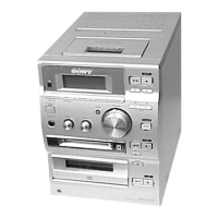
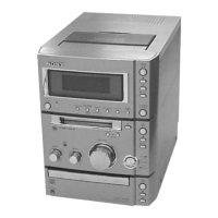
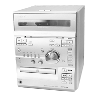
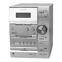
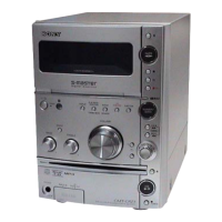
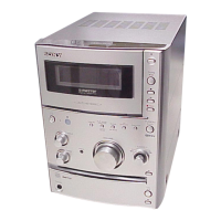
HCD-CP500K/CP500MD
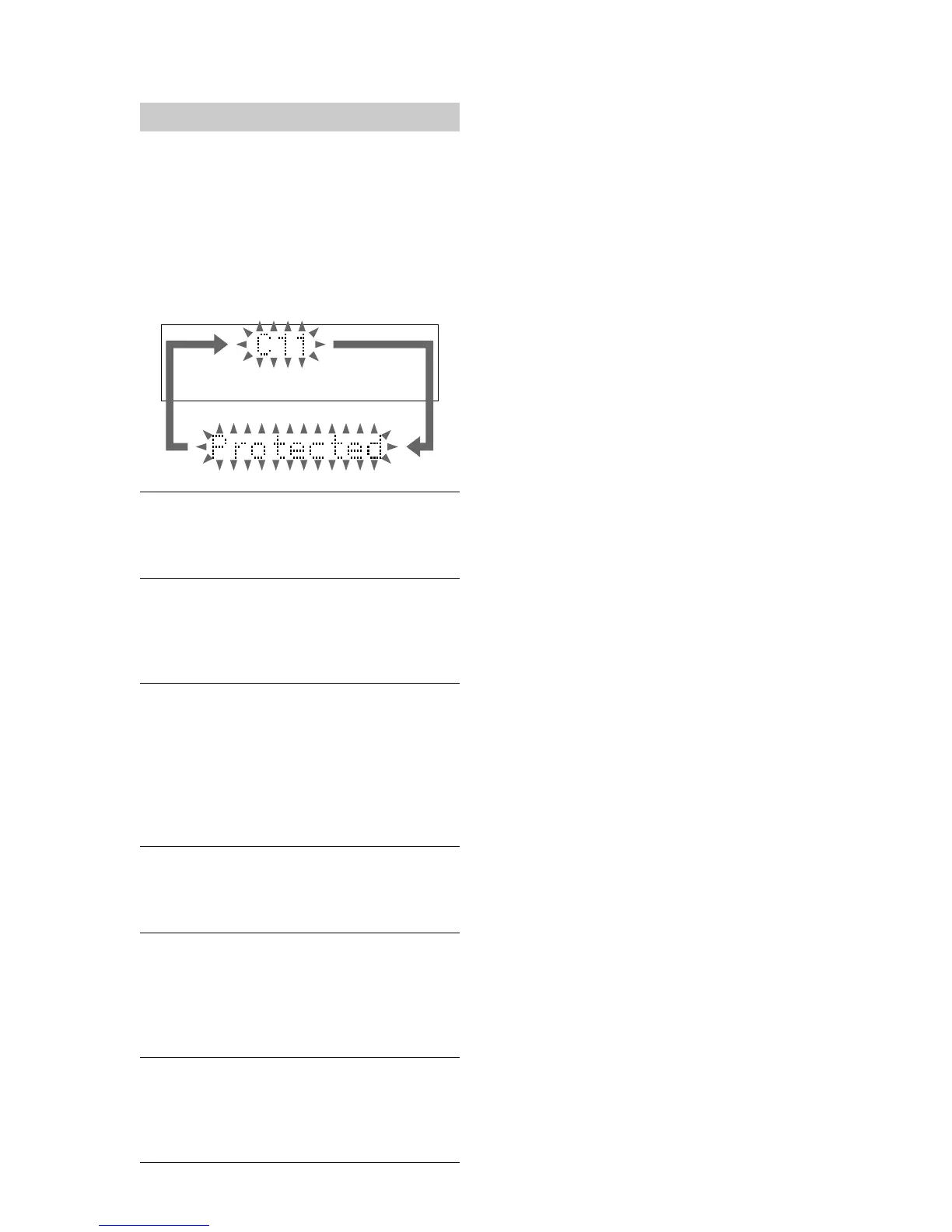
Self-diagnosis display
This system has a Self-diagnosis display
function to let you know if there is a system
malfunction. The display shows a code made
up of three letters and a message alternately to
show you the problem. To solve the problem
refer to the following list. If any problem
persists, consult your nearest Sony dealer.
C11/Protected
The MD is protected against erasure.
Remove the MD and slide the tab to close the
slot (see page 16).
C12/Cannot Copy
You tried to record a CD or MD with a format that
the system does not support, such as a CD-ROM.
p Remove the disc and turn off the system once,
then turn it on again.
C13/REC Error
Recording could not be performed properly.
p Move the system to a stable place, and start
recording over from the beginning.
The MD is dirty or scratched, or the MD does not
meet the standards.
p Replace the MD and start recording over from
the beginning.
C13/Read Error
The MD deck cannot read the disc information
properly.
p Remove the MD once, then load it again.
C14/Toc Error
The MD deck cannot read the disc information
properly.
p Replace the MD.
p Erase all the recorded contents of the MD using
All Erase Function (see page 27).
C41/Cannot Copy
The sound source is a copy of commercially
available music software.
p The Serial Copy Management System prevents
making a digital copy (see page 47).
1. SERVICING NOTES ······················································ 4
2. GENERAL ·········································································· 9
3. DISASSEMBLY ······························································ 11
4. TEST MODE··································································· 20
5. MECHANICAL ADJUSTMENTS ···························· 26
6. ELECTRICAL ADJUSTMENTS ······························ 26
7. DIAGRAMS
7-1. CIRCUIT BOARDS LOCATIONS ··································· 41
7-2. BLOCK DIAGRAM – CD SECTION – ··························· 42
BLOCK DIAGRAM – MAIN SECTION – ······················ 43
BLOCK DIAGRAM – MD SECTION – ·························· 44
BLOCK DIAGRAM – PANEL SECTION – ···················· 45
7-3. PRINTED WIRING BOARD – CD BOARD – ················ 46
7-4. SCHEMATIC DIAGRAM – CD BOARD – ····················· 47
7-5. PRINTED WIRING BOARD – BD BOARD – ················ 48
7-6. SCHEMATIC DIAGRAM – BD BOARD (1/2) – ············ 49
7-7. SCHEMATIC DIAGRAM – BD BOARD (2/2) – ············ 50
7-8. PRINTED WIRING BOARDS – AUDIO SECTION – ···· 51
7-9. SCHEMATIC DIAGRAM – AUDIO SECTION (1/2) –··· 52
7-10.SCHEMATIC DIAGRAM – AUDIO SECTION (2/2) –··· 53
7-11.PRINTED WIRING BOARD – TC BOARD – ················· 54
7-12.SCHEMATIC DIAGRAM – TC BOARD – ······················ 55
7-13.PRINTED WIRING BOARD – DIGITAL BOARD – ······ 56
7-14 SCHEMATIC DIAGRAM – DIGITAL BOARD – ··········· 57
7-15.
PRINTED WIRING BOARDS – CONTROL SECTION –
··· 58
7-16 SCHEMATIC DIAGRAM – CONTROL BOARD – ········ 59
7-17.PRINTED WIRING BOARD – POWER BOARD – ········ 60
7-18.SCHEMATIC DIAGRAM – POWER BOARD – ············· 60
7-19.IC BLOCK DIAGRAMS ·················································· 61
7-20.IC Pin Function Description ·············································· 63
8. EXPLODED VIEWS ····················································· 71
9. ELECTRICAL PARTS LIST····································· 78
TABLE OF CONTENTS
 Loading...