EasyManua.ls Logo

Sony HCD-CP33 Service Manual

Sony HCD-CP33
84 pages
To Next Page IconTo Next Page
Page #1 background imageLoading...
Page #1 background image
HCD-CP33
US Model
Canadian Model
AEP Model
UK Model
E Model
Australian Model
Tourist Model
SERVICE MANUAL
MICRO Hi-Fi COMPONENT SYSTEM
— Continued on next page —
SPECIFICATIONS
Dolby noise reduction manufactured under license
from Dolby Laboratories Licensing Corporation.
“DOLBY” and the double-D symbol a are trade-
marks of Dolby Laboratories Licensing Corporation.
HCD-CP33 is the Amplifier, MD player,
CD player, Tape Deck and Tuner section
in CMT-CP33MD.
Note
CD block, tape deck block and
tuner pack are supplied with
the assembled block.
Amplifier section
For the U.S. model
AUDIO POWER SPECIFICATIONS
POWER OUTPUT AND TOTAL HARMONIC
DISTORTION:
With 6- loads, both channels driven, from
70 – 20,000 Hz; rated 18 W per channel
minimum RMS power, with no more than 0.9%
total harmonic distortion from 250 mW to
rated output.
North American model:
Continuous RMS power output (reference):
35 + 35 W
(6 at 1 kHz, 10% THD)
Total harmonic distortion: less than 0.07%
(6 at 1 kHz, 18 W)
European model:
DIN power output (Rated):30 + 30 W
(6 at 1 kHz, DIN, 230 V)
Continuous RMS power output (Reference):
35 + 35 W
(6 at 1 kHz,10% THD, 230 V)
Music power output (Reference):
85 + 85 W
Other models:
The following measured at 230 V AC, 60 Hz
DIN power output (rated): 28 + 28 W
(6 at 1 kHz, DIN)
Continuous RMS power output (reference):
30 + 30 W
(6 at 1 kHz, 10% THD)
The following measured at 220 V AC, 60 Hz
DIN power output (rated): 24 + 24 W
(6 at 1 kHz, DIN)
Continuous RMS power output (reference):
25 + 25 W
(6 at 1 kHz, 10% THD)
Inputs
VIDEO IN (phono jacks): voltage 250 mV, impedance 47 k
Outputs
LINE OUT (phono jack): voltage 250 mV, impedance 1 k
PHONES (stereo minijack):
accepts headphones of 8 ormore.
SPEAKER: accepts impedance of 6 to16
CD player section
System Compact disc and digital audio
system
Laser Semiconductor laser (l=780 nm)
Emission duration: continuous
Laser output Max. 44.6 µW*
*This output is the value measured
at a distance of 200 mm from the
objective lens surface on the
Optical Pick-up Block with 7 mm
aperture.
Frequency response 2 Hz – 20 kHz
Model Name Using Similar Mechanism HCD-CP11
CD Mechanism Type CDM55-K5BD41
Model Name Using Similar Mechanism HCD-MDX10
Mechanism Type MDM-5A
Optical Pick-up Type KMS-260A/K1NP
Model Name Using Similar Mechanism HCD-CP11
Tape Transport Mechanism Type TCB-020
CD
Section
MD
Section
Tape deck
Section
Ver 1.2 2003. 05
Sony Corporation
Home Audio Company
Published by Sony Engineering Corporation
9-929-276-13
2003E16-1
© 2003.05
Question and Answer IconNeed help?

Do you have a question about the Sony HCD-CP33 and is the answer not in the manual?

Sony HCD-CP33 Specifications

General IconGeneral
CD PlayerYes
Speakers2-way speakers
Number of Discs1
Remote ControlYes
TypeMini HiFi System
InputsAudio in
Tuner BandsFM, AM
Speakers TypeBass Reflex
TunerAM/FM

Summary

Sony HCD-CP33 Service Manual Overview

HCD-CP33 Technical Specifications

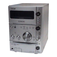
Lists detailed technical specifications for the HCD-CP33 unit, including power, inputs, and outputs.

Disassembly Procedures for HCD-CP33

Servicing Notes and Safety Precautions

AC Leakage Testing Procedures

Instructions for checking AC leakage from exposed metal parts.

Safety Checks Post-Repair

Essential safety checks to perform before releasing the unit to customers.

HCD-CP33 Service Mode Operations

Panel Test Mode Entry

Procedure for entering the Panel Test Mode.

Tape Deck Aging Mode Procedure

Steps to activate and use the Tape Deck Aging Mode.

CD Aging Mode Activation

Procedure for entering and utilizing the CD Aging Mode.

Cold Reset Procedure

Instructions for performing a cold reset to clear memory.

Hot Reset Procedure

Steps to perform a hot reset while retaining memory data.

MD Test Mode Procedures

Test Mode Usage Precautions

Important safety and operational precautions before using MD test modes.

Setting the MD Test Mode

Methods for entering specific test modes for the MD section.

Selecting and Operating MD Test Modes

Test Mode Selection Guide

Details on how to navigate and select various service test modes.

MD Continuous Playback and Recording

Electrical Adjustments for HCD-CP33

MD Section Parts Replacement and Adjustment Flow

Flowchart guiding parts replacement and adjustment in the MD section.

Laser and Optical Pick-Up Precautions

Laser Diode Emission Check Precautions

Safety warnings for checking laser diode emission.

Optical Pick-Up Handling Precautions

Specific precautions for handling the optical pick-up unit.

General Adjustment Precautions

Important precautions to follow before performing any adjustments.

Pre-Repair Checks and Adjustments

Temperature Compensation Offset Check

Procedure to check the temperature compensation offset.

Initial Setting and Offset Adjustments

Initial Setting of Adjustment Value

Procedure to reset all adjustments to their initial values.

Recording and Displaying IOP Information

Process for recording and displaying optical pick-up IOP data.

Temperature Compensation Offset Adjustment

Procedure to adjust the temperature compensation offset.

Laser Power and Traverse Adjustments

Laser Power Adjustment Procedure

Steps for adjusting the laser power output.

Traverse Adjustment Procedure

Instructions for adjusting the traverse mechanism.

Focus Bias Adjustment Procedure

Focus Bias Adjustment Steps

Detailed steps for performing the focus bias adjustment.

Error Rate and Auto Gain Adjustments

Deck Section Adjustments

Diagrams and Notes

Block Diagrams

BD Section Block Diagram

Functional block diagram of the BD section.

Main Section Block Diagram

Main Section Functional Blocks

Block diagram illustrating the main section's components and connections.

Power Section Block Diagram

Power Section Functional Blocks

Block diagram detailing the power supply section.

BD Section Schematic Diagrams

BD Schematic Diagram (1/2)

Schematic diagram for the BD board, part 1.

BD Section Schematic Diagram (Part 2)

BD Schematic Diagram (2/2)

Schematic diagram for the BD board, part 2.

BD Section Printed Wiring Boards

Main Section Printed Wiring Boards

Main Section Schematic Diagrams

Main Schematic Diagram (1/2)

Schematic diagram for the main section, part 1.

Main Section Schematic Diagram (Part 2)

Main Schematic Diagram (2/2)

Schematic diagram for the main section, part 2.

Control Section Diagrams

Control Section Schematic Diagram

Control Section Schematic

Schematic diagram for the control section.

Digital Section Printed Wiring Board

Digital Section Schematic Diagram

Digital Board Schematic

Schematic diagram for the digital board.

Power Section Printed Wiring Board

Power Section Schematic Diagram

Power Board Schematic

Schematic diagram for the power supply board.

IC Pin Functions for HCD-CP33

IC121 Pin Functions

IC306 System Control Pin Functions

Exploded Views of HCD-CP33 Components

Electrical Parts List - BD Board

Related product manuals