HCD-CX4iP/CX5iP
39
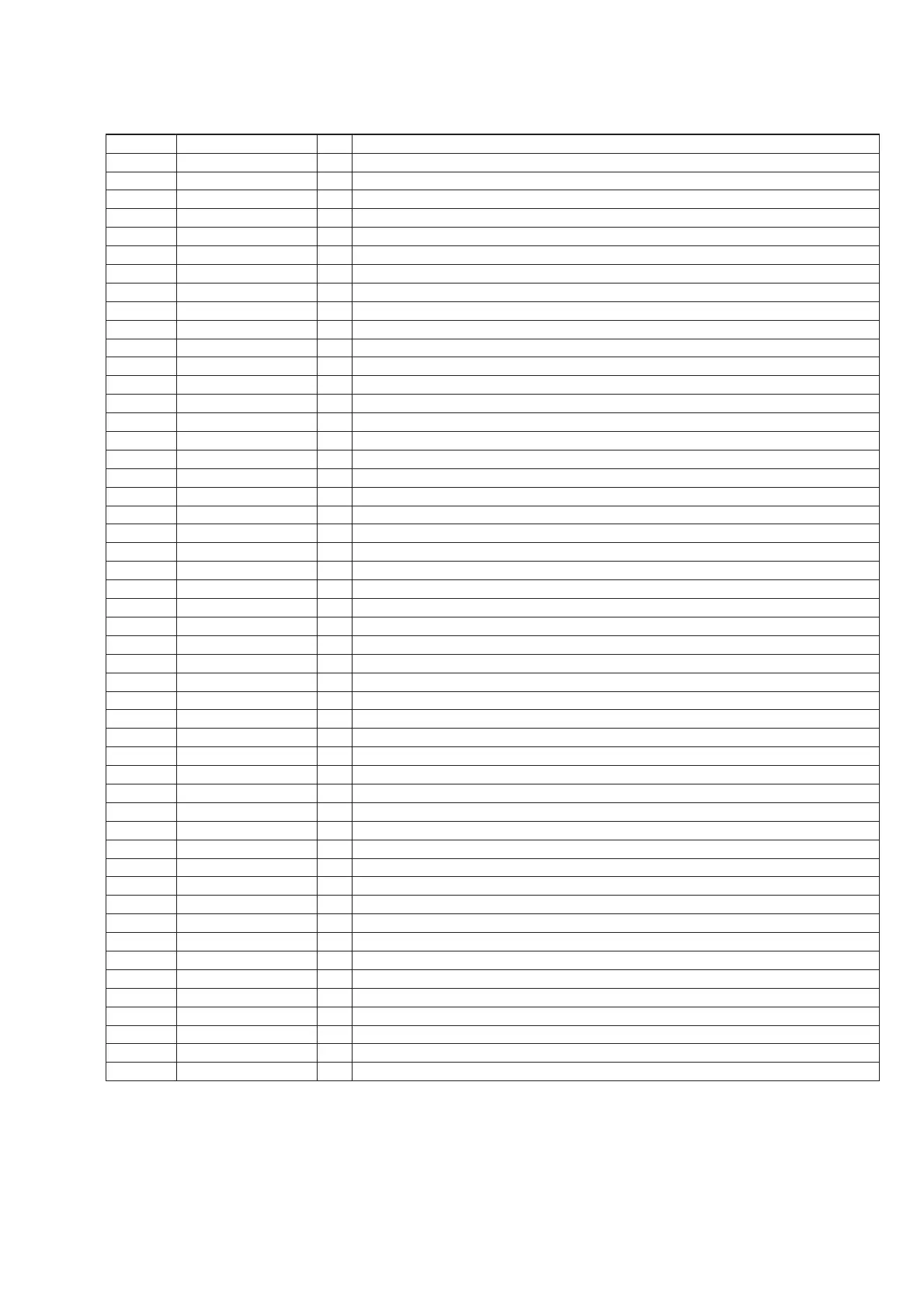
MAIN BOARD IC601 BU9408KS2 (DSP)
Pin No. Pin Name I/O Description
1 DVDDPLL - Power supply terminal (+3.3V)
2 FILT1 - Not used
3 DGNDPLL - Ground terminal
4 FILT2 - Not used
5 SCANTEST - Not used
6 I2CADR - Not used
7 SCL I Serial data transfer clock signal input from the system controller
8 SDA I/O Serial data input/output with the system controller
9 DGNDIO1 - Ground terminal
10 RESETB I Reset signal input from the system controller
11 DVDDCOR1 - Connect to pin 37
12 MUTE1B I Muting on/off control signal input from the system controller
13, 14 MUTE2B, MUTE3B I Muting on/off control signal input terminal Not used
15 AGNDDA1 - Ground terminal
16 AOUTR1 - Not used
17 AOUTL1 O Audio level detection signal output to the system controller
18, 19 AVDDDA1, AVDDDA2 - Power supply terminal (+3.3V)
20 AOUTR2 - Not used
21 VREFDA - Not used
22 AOUTL2 - Not used
23 AGNDDA2 - Ground terminal
24 ERR1_LRC - Not used
25 ERR2_BCK - Not used
26 DATASO - Not used
27 DATAMO O Audio data output to the power amplifi er
28 BCKO O Bit clock signal output to the power amplifi er
29 LRCKO O L/R sampling clock signal output to the power amplifi er
30 AMCLKO O Master clock signal output to the A/D converter and power amplifi er
31 SPDIFO - Not used
32 DGNDIO2 - Ground terminal
33 XI I System clock input terminal (24.576 MHz)
34 XO O System clock output terminal (24.576 MHz)
35 DVDDIO - Power supply terminal (+3.3V)
36 ANATEST - Not used
37 DVDDCOR2 - Connect to pin 11
38 DVDDREG - Power supply terminal (+3.3V)
39 LDOPOFF - Not used
40 DGNDREG - Ground terminal
41 LRCKI1 I L/R sampling clock signal input from the A/D converter
42 BCKI1 I Bit clock signal input from the A/D converter
43 DATAI1 I Audio data input from the A/D converter
44 LRCKI2 I L/R sampling clock signal input terminal Not used
45 BCKI2 I Bit clock signal input terminal Not used
46 DATAI2 I Audio data input terminal Not used
47 LRCKI3 I L/R sampling clock signal input from the DSP
48 BCKI3 I Bit clock signal input from the DSP
49 DATAI3 I Audio data input from the DSP
50 LRCKI4 I L/R sampling clock signal input from the CD-MP3 processor
51 BCKI4 I Bit clock signal input from the CD-MP3 processor
52 DATAI4 I Audio data input from the CD-MP3 processor
 Loading...