EasyManua.ls Logo

Sony HCD-DX155 User Manual

Sony HCD-DX155
92 pages
To Next Page IconTo Next Page
Page #1 background imageLoading...
Page #1 background image
SERVICE MANUAL
Sony Corporation
Home Audio Division
Published by Sony Techno Create Corporation
US Model
Canadian Model
HCD-DX155/DX255
E Model
Australian Model
HCD-DX155
SUPER AUDIO CD/DVD RECEIVER
9-887-098-03
2006D16-1
© 2006.04
Ver. 1.2 2006.04
HCD-DX155/DX255
HCD-DX155/DX255 are the amplifier, DVD/CD
and tuner section in DAV-DX155/DX255.
SPECIFICATIONS
Model Name Using Similar Mechanism HCD-DX150
Mechanism Type CDM81C-DVBU101
Optical Pick-up Name
KHM-310CAB
This system incorporates with Dolby*
1
Digital and Dolby Pro Logic (II)
adaptive matrix surround decoder and the DTS*
2
Digital Surround
System.
*1 Manufactured under license from Dolby Laboratories.
“Dolby,” “Pro Logic,” and the double-D symbol are trademarks of
Dolby Laboratories.
*2 Manufactured under license from Digital Theater Systems, Inc.
“DTS” and “DTS Digital Surround” are trademarks of Digital
Theater Systems, Inc.
— Continued on next page —
Photo : HCD-DX255
AUDIO POWER SPECIFICATIONS
for the US model
DX155
POWER OUTPUT AND
TOTAL HARMONIC
DISTORTION
(FTC Output Power): FL/FR/LS/RS/C: 84 W/ch
3 ohm at 170 - 20,000 Hz,
0.7 % THD
SW: 80 W 3 ohm at 40 -
170 Hz, 0.7 % THD
DX255
POWER OUTPUT AND
TOTAL HARMONIC
DISTORTION
(FTC Output Power): FL/FR/LS/RS/C: 84 W/ch
3 ohm at 170 - 20,000 Hz,
0.7 % THD
SW: 160 W 1.5 ohm at 40 -
170 Hz, 0.7 % THD
Amplifier section
DX155
US models:
Surround mode (reference)
RMS output power, 10 %
THD
Front: 142 W + 142 W
(with SS-TS52)
Center*: 142 W
(with SS-CT51)
Surround*: 142 W + 142
W
(with SS-TS51)
Subwoofer*: 140 W
(with SS-WS52)
Mexican and other models:
Stereo mode (rated) 108 W + 108 W (3 ohms at
1 kHz, 1 % THD)
Surround mode (reference)
RMS output power, 10 %
THD
Front: 142 W + 142 W
(with SS-TS52)
Center*: 142 W
(with SS-CT51)
Surround*: 142 W + 142
W
(with SS-TS51)
Subwoofer*: 140 W
(with SS-WS52)
Latin American models:
Stereo mode (rated) 100 W + 100 W (3 ohms at
1 kHz, 1 % THD)
Surround mode (reference)
RMS output power, 10 %
THD
Front: 133 W + 133 W
(with SS-TS52)
Center*: 133 W
(with SS-CT51)
Surround*: 133 W + 133
W
(with SS-TS51)
Subwoofer*: 135 W
(with SS-WS52)
DX255
US models:
Surround mode (reference)
RMS output power, 10 %
THD
Front: 143 W + 143 W
(with SS-TS52)
Center*: 143 W
(with SS-CT51)
Surround*: 143 W + 143
W
(with SS-TS51)
Subwoofer*: 285 W
(with SS-WS52B)

Table of Contents

Question and Answer IconNeed help?

Do you have a question about the Sony HCD-DX155 and is the answer not in the manual?

Sony HCD-DX155 Specifications

General IconGeneral
BrandSony
ModelHCD-DX155
CategoryReceiver
LanguageEnglish

Summary

SPECIFICATIONS

AUDIO POWER SPECIFICATIONS

Details audio power output and total harmonic distortion for US models DX155 and DX255.

MODEL IDENTIFICATION

Rear Panel

Identifies connectors and features on the rear panel of the unit.

SAFETY CHECK-OUT

LEAKAGE TEST

Procedure for testing AC leakage from exposed metal parts to earth ground.

Unleaded Solder

Characteristics and handling of unleaded solder.

SECTION 1 SERVICING NOTE

NOTES ON HANDLING THE OPTICAL PICK-UP BLOCK OR BASE UNIT

Precautions for handling the optical pick-up block and its flexible board.

Self-diagnosis Function

Explanation of service numbers and their corrective actions.

Discharge the charged electricity in capacitors to prevent electric shock as follows

POWER board

Capacitors on the POWER board that need discharging.

Fix the capacitors with adhesive agent as follows

PRECAUTION WHEN INSTALLING A NEW OP UNIT / PRECAUTION BEFORE UNSOLDERING THE STATIC ELECTRICITY PREVENTION SOLDER BRIDGE

Important precautions for installing a new OP unit and handling static electricity.

SECTION 2 GENERAL

Front panel

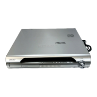
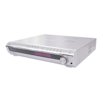
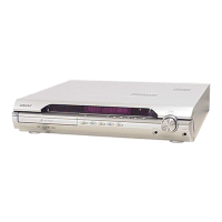
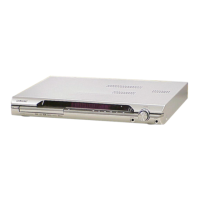
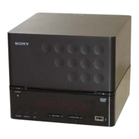
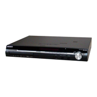
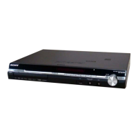
Identification of controls and indicators on the front panel.

Rear panel

Identification of connectors and inputs/outputs on the rear panel.

Front panel display

About the indications in the front panel display

Explanation of the symbols and indicators shown on the front panel display.

Remote control

BUTTON DESCRIPTIONS

Description of the functions for each button on the remote control.

SECTION 3 DISASSEMBLY

3-1. DISASSEMBLY FLOW

Flowchart illustrating the sequence of disassembly steps for the unit.

3-2. CASE, FRONT PANEL ASSY

how to open the disc table when power switch turns off

Procedure to open the disc table mechanism when the power is off.

3-3. FL BOARD, SW BOARD

3-4. JACK BOARD, LED BOARD

3-5. I/O BOARD, TUNER

3-6. SPEAKER BOARD, D.C. FAN

3-7. MAIN BOARD

3-8. POWER BOARD

INSTALLING THE POWER BOARD

Procedure for installing the power board for specific models.

3-9. DVD MECHANISM DECK (CDM81C-DVBU101)

3-10. TRAY

3-11. MOTOR BOARD M761 (LD/ST MOTOR), M762 (BU U/D MOTOR)

3-12. BASE UNIT (DVBU101)

3-13. OPTICAL PICK-UP (KHM-310CAB)

3-14. GEAR (SUB TRAY 1), GEAR (SUB TRAY 2)

PRECAUTION DURING GEAR (SUB TRAY 1/2) INSTALLATION

Precautions for installing gears for sub tray 1 and 2.

3-15. LEVER ASSY

Before re-assembling, slide the cam (BU) in the direction of the arrow.

Slide cam (BU) in the specified direction before re-assembly.

3-16. STOCKER SECTION

Rotate the gear (SS3) in the direction of the arrow.

Rotate the gear (SS3) in the direction indicated by the arrow.

3-17. CAM (STOCKER)

PRECAUTION DURING CAM (STOCKER) INSTALLATION

Precautions for installing cams (stocker).

3-18. GEAR (STOCKER 3)

PRECAUTION DURING GEAR (STOCKER 3) INSTALLATION

Precautions for installing the gear (stocker 3).

3-19. ROTARY ENCODER (MD)

PRECAUTION DURING ROTARY ENCODER (MD) INSTALLATION

Precautions for installing the rotary encoder (MD).

3-20. GEAR (BU1)

PRECAUTION DURING GEAR (BU1) INSTALLATION

Precautions for installing the gear (BU1).

SECTION 4 TEST MODE

1. Cold Reset

Clears all data, including preset data, to initial conditions.

4. DVD Ship Mode

Prepares the set for shipping after repair.

DVD SECTION

8-2. HOW TO ENTER TEST MODE

Procedure to enter test mode using specific button combinations.

8-4. MIRROR TIME ADJUSTMENT

Menu for checking and adjusting CD and DVD mirror times.

8-4-1. EXECUTING MIRROR TIME ADJUSTMENT

(14) Confirm the same values are displayed. If it is not same, return to step 7.

Confirms saved values and returns to step 7 if inconsistent.

(22) Confirm the same values are displayed. If it is not the same, return to step 15.

Confirms saved values and returns to step 15 if inconsistent.

8-5. EXECUTING IOP MEASUREMENT

SECTION 5 ELECTRICAL ADJUSTMENT

[RF Level Check]

Checks the RF signal level.

SECTION 6 DIAGRAMS

Circuit Boards Location

Diagram showing the location of various circuit boards within the unit.

6-1. BLOCK DIAGRAM - RF SECTION -

Signal Path

Diagram illustrating signal paths for CD, DVD, and SACD playback.

6-2. BLOCK DIAGRAM - AMP SECTION -

Signal Path

Diagram illustrating signal paths for audio and tuner inputs.

6-3. BLOCK DIAGRAM - AUDIO SECTION -

Signal Path

Diagram illustrating signal paths for audio processing and output.

6-4. BLOCK DIAGRAM - VIDEO SECTION -

Signal Path

Diagram illustrating signal paths for video and component video outputs.

6-5. BLOCK DIAGRAM - POWER SECTION -

6-6. PRINTED WIRING BOARD - MAIN BOARD (SIDE A) -

Semiconductor Location

Table listing semiconductor reference numbers and their locations on the MAIN board.

6-8. SCHEMATIC DIAGRAM - MAIN BOARD (1/10) -

6-18. PRINTED WIRING BOARD - I/O BOARD

Semiconductor Location

Table listing semiconductor reference numbers and their locations.

6-20. PRINTED WIRING BOARDS - PANEL SECTION

【FL BOARD】

Printed wiring board layout for the FL display.

【JACK BOARD】

Printed wiring board layout for the jack board.

【LED BOARD】

Printed wiring board layout for the LED board.

【SW BOARD】

Printed wiring board layout for the SW board.

6-21. SCHEMATIC DIAGRAM - PANEL SECTION

【LED BOARD】

Schematic diagram for the LED board.

【JACK BOARD】

Schematic diagram for the jack board.

【FL BOARD】

Schematic diagram for the FL board.

【SW BOARD】

Schematic diagram for the SW board.

6-22. PRINTED WIRING BOARD - SPEAKER BOARD

【SPEAKER BOARD】

Printed wiring board layout for the speaker board.

6-23. SCHEMATIC DIAGRAM - SPEAKER BOARD

【SPEAKER BOARD】

Schematic diagram for the speaker board.

6-24. PRINTED WIRING BOARDS - CD MECHANISM SECTION

【MOTOR BOARD】

Printed wiring board layout for the motor board.

【SENSOR BOARD】

Printed wiring board layout for the sensor board.

【RELAY BOARD】

Printed wiring board layout for the relay board.

【SW (1) BOARD】

Printed wiring board layout for the SW (1) board.

【SW (2) BOARD】

Printed wiring board layout for the SW (2) board.

【ENCODER BOARD】

Printed wiring board layout for the encoder board.

Semiconductor Location

Table listing semiconductor reference numbers and their locations.

6-25. SCHEMATIC DIAGRAM - CD MECHANISM SECTION

【RELAY BOARD】

Schematic diagram for the relay board.

【MOTOR BOARD】

Schematic diagram for the motor board.

【SW (1) BOARD】

Schematic diagram for the SW (1) board.

【SW (2) BOARD】

Schematic diagram for the SW (2) board.

【SENSOR BOARD】

Schematic diagram for the sensor board.

6-26. PRINTED WIRING BOARD - POWER BOARD

【POWER BOARD】

Printed wiring board layout for the power board.

Semiconductor Location

Table listing semiconductor reference numbers and their locations.

6-27. SCHEMATIC DIAGRAM - POWER BOARD

Waveforms

MAIN Board - IC1101 (DVDRFIP)

Waveform details for IC1101 on the MAIN board.

I/O Board - IC201 (CVBS)

Waveform details for IC201 on the I/O board.

IC Block Diagrams - MAIN Board - IC2200 PCM1803DBR

Block diagram for IC2200 on the MAIN board.

IC Block Diagrams - MAIN Board - IC3010, IC3020, IC3030 CXD9788AR

Block diagrams for IC3010, IC3020, IC3030 on the MAIN board.

IC Block Diagrams

MAIN Board IC3050 TK11118CSCL-G

Block diagram for IC3050 on the MAIN board.

I/O Board - IC201 MM1623BFBE

Block diagram for IC201 on the I/O board.

I/O Board - IC352 MC14052BDR2

Block diagram for IC352 on the I/O board.

LED Board - IC803 BU2099FV

Block diagram for IC803 on the LED board.

IC Block Diagrams

FL Board - IC802 PT6315

Block diagram for IC802 on the FL board.

RELAY Board - IC701, IC711 BA6956AN

Block diagrams for IC701 and IC711 on the RELAY board.

IC Pin Function Description

MAIN BOARD IC501 M30622MEP-A61FPU0 (SYSTEM CONTROLLER)

Pin function description for IC501 on the MAIN board.

MAIN BOARD IC501 M30622MEP-A61FPU0 (SYSTEM CONTROLLER)

Pin No. Pin Name I/O Description

Detailed pin information for IC501.

MAIN BOARD IC501 M30622MEP-A61FPU0 (SYSTEM CONTROLLER)

Pin No. Pin Name I/O Description

Detailed pin information for IC501.

MAIN BOARD IC1101 CXD9849R (CD/DVD RF AMP, FOCUS/TRACKING ERR AMP, DVD SYSTEM PROCESSOR, DIGITAL SERVO PROCESSOR)

Pin No. Pin Name I/O Description

Pinout and description for IC1101 on the MAIN board.

MAIN BOARD IC1101 CXD9849R (CD/DVD RF AMP, FOCUS/TRACKING ERR AMP, DVD SYSTEM PROCESSOR, DIGITAL SERVO PROCESSOR)

Pin No. Pin Name I/O Description

Pinout and description for IC1101 on the MAIN board.

MAIN BOARD IC1101 CXD9849R (CD/DVD RF AMP, FOCUS/TRACKING ERR AMP, DVD SYSTEM PROCESSOR, DIGITAL SERVO PROCESSOR)

Pin No. Pin Name I/O Description

Pinout and description for IC1101 on the MAIN board.

MAIN BOARD IC1101 CXD9849R (CD/DVD RF AMP, FOCUS/TRACKING ERR AMP, DVD SYSTEM PROCESSOR, DIGITAL SERVO PROCESSOR)

Pin No. Pin Name I/O Description

Pinout and description for IC1101 on the MAIN board.

MAIN BOARD IC1101 CXD9849R (CD/DVD RF AMP, FOCUS/TRACKING ERR AMP, DVD SYSTEM PROCESSOR, DIGITAL SERVO PROCESSOR)

Pin No. Pin Name I/O Description

Pinout and description for IC1101 on the MAIN board.

SECTION 7 EXPLODED VIEWS

7-1. OVERALL SECTION

Exploded view of the overall unit assembly.

7-2. FRONT PANEL SECTION

7-3. CHASSIS SECTION

7-4. DVD MECHANISM DECK SECTION-1 (CDM81C-DVBU101)

7-5. DVD MECHANISM DECK SECTION-2 (CDM81C-DVBU101)

7-6. DVD MECHANISM DECK SECTION-3 (CDM81C-DVBU101)

7-7. BASE UNIT (DVBU101)

SECTION 8 ELECTRICAL PARTS LIST

< CAPACITOR >

List of capacitors with part numbers and specifications.

< RESISTOR >

List of resistors with part numbers and specifications.

< DIODE >

List of diodes with part numbers and specifications.

SECTION 8 ELECTRICAL PARTS LIST

< TRANSFORMER >

List of transformers with part numbers and specifications.

< CAPACITOR >

List of capacitors with part numbers and specifications.

< TRANSISTOR >

List of transistors with part numbers and specifications.

< RESISTOR >

List of resistors with part numbers and specifications.

SECTION 8 ELECTRICAL PARTS LIST

< DIODE >

List of diodes with part numbers and specifications.

< FERRITE BEAD >

List of ferrite beads with part numbers and specifications.

< IC >

List of integrated circuits with part numbers and specifications.

< JACK >

List of jacks with part numbers.

< SHORT >

List of short circuit components.

< TRANSISTOR >

List of transistors with part numbers and specifications.

< RESISTOR >

List of resistors with part numbers and specifications.

JACK LED

< TRANSISTOR >

List of transistors with part numbers and specifications.

< RESISTOR >

List of resistors with part numbers and specifications.

< SWITCH >

List of switches with part numbers and functions.

MAIN

< CAPACITOR >

List of capacitors with part numbers and specifications.

MAIN

< CAPACITOR >

List of capacitors with part numbers and specifications.

MAIN

< CAPACITOR >

List of capacitors with part numbers and specifications.

POWER

< DIODE >

List of diodes with part numbers and specifications.

< GROUND TERMINAL BOARD >

List of ground terminal boards with part numbers.

< FUSE HOLDER >

List of fuse holders with part numbers.

< FUSIBLE >

List of fusible components with part numbers.

< IC >

List of integrated circuits with part numbers and specifications.

< COIL >

List of coils with part numbers and specifications.

MAIN

< TRANSISTOR >

List of transistors with part numbers and specifications.

< SHORT >

List of short circuit components.

< COIL >

List of coils with part numbers and specifications.

MAIN

< TRANSISTOR >

List of transistors with part numbers and specifications.

< RESISTOR >

List of resistors with part numbers and specifications.

MAIN

< RESISTOR >

List of resistors with part numbers and specifications.

MAIN

< RESISTOR >

List of resistors with part numbers and specifications.

MAIN MOTOR POWER

< NETWORK RESISTOR >

List of network resistors with part numbers and specifications.

MOTOR BOARD

Part number for the motor board.

< SWITCH >

List of switches with part numbers and functions.

POWER BOARD, COMPLETE

Part number for the complete power board.

< CAPACITOR >

List of capacitors with part numbers and specifications.

POWER

< DIODE >

List of diodes with part numbers and specifications.

< GROUND TERMINAL BOARD >

List of ground terminal boards with part numbers.

< FUSE HOLDER >

List of fuse holders with part numbers.

< FUSIBLE >

List of fusible components with part numbers.

< IC >

List of integrated circuits with part numbers and specifications.

< COIL >

List of coils with part numbers and specifications.

POWER

< LINE FILTER >

List of line filters with part numbers.

< IC >

List of integrated circuits with part numbers and specifications.

< TRANSISTOR >

List of transistors with part numbers and specifications.

< RESISTOR >

List of resistors with part numbers and specifications.

< TRANSFORMER >

List of transformers with part numbers and specifications.

< THERMISTOR >

List of thermistors with part numbers.

< VARISTOR >

List of varistors with part numbers.

RELAY SENSOR SPEAKER SW SW (1) SW (2)

< CAPACITOR >

List of capacitors with part numbers and specifications.

< CONNECTOR >

List of connectors with part numbers.

< DIODE >

List of diodes with part numbers and specifications.

< IC >

List of integrated circuits with part numbers and specifications.

< TRANSISTOR >

List of transistors with part numbers and specifications.

< RESISTOR >

List of resistors with part numbers and specifications.

SENSOR BOARD

Parts list for the sensor board.

< IC >

List of integrated circuits with part numbers and specifications.

SPEAKER BOARD

Parts list for the speaker board.

< CAPACITOR >

List of capacitors with part numbers and specifications.

< CONNECTOR >

List of connectors with part numbers.

< GROUND TERMINAL BOARD >

List of ground terminal boards with part numbers.

< TERMINAL >

List of terminal boards with part numbers.

SW BOARD

Parts list for the SW board.

< SWITCH >

List of switches with part numbers and functions.

SW (1) BOARD

Parts list for the SW (1) board.

< SWITCH >

List of switches with part numbers and functions.

SW (2) BOARD

Parts list for the SW (2) board.

< SWITCH >

List of switches with part numbers and functions.

MISCELLANEOUS

List of miscellaneous parts.

REVISION HISTORY

Ver. Date Description of Revision

History of revisions made to the service manual.

Related product manuals