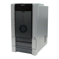
104
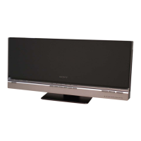
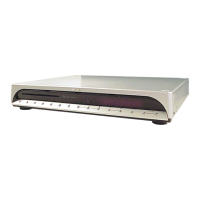
HCD-FLX5D/FLX7D
MB BOARD IC801 CXD2752R (DSD DECODER) (FLX7D only)
Pin No. Pin Name I/O Description
1 VSCA0 —
Ground terminal (for core)
2 XMSLAT I
Serial data latch pulse signal input from the mechanism controller
3 MSCK I
Serial data transfer clock signal input from the mechanism controller
4 MSDATI I
Serial data input from the mechanism controller
5 VDCA0 —
Power supply terminal (+2.5V) (for core)
6 MSDATO O
Serial data output to the mechanism controller
7 MSREADY O
Ready signal output to the mechanism controller “L”: ready
8 XMSDOE O
Serial data output enable signal output terminal Not used
9 XRST I
Reset signal input from the mechanism controller “L”: reset
10 SMUTE I
Soft muting on/off control signal input from the mechanism controller “H”: muting on
11 MCKI I
Master clock signal (33.8688 MHz) input
12 VSIOA0 —
Ground terminal (for I/O)
13 EXCKO1 O
Master clock signal (33.8688 MHz) output to the digital audio processor
14 EXCKO2 O
External clock 2 signal output terminal Not used
15 LRCK O
L/R sampling clock signal (44.1kHz) output terminal Not used
16 F75HZ O
Not used
17 VDIOA0 —
Power supply terminal (+3.3V) (for I/O)
18 to 25 MNT0 to MNT7 O
Monitor signal output terminal Not used
26 TCK I
Clock signal input from the DVD system processor
27 TDI I
Serial data input from the DVD system processor
28 VSCA1 —
Ground terminal (for core)
29 TDO O
Serial data output terminal Not used
30 TMS I
MS signal input from the DVD system processor
31 TRST I
Reset signal input from the DVD system processor “L”: reset
32 to 34 TEST1 to TEST3 I
Input terminal for the test (normally: fixed at “L”)
35 VDCA1 —
Power supply terminal (+2.5V) (for core)
36 UBIT O
Not used
37 XBIT O
Not used
38 to 41
SUPDT0 to
SUPDT3
O
Supplementary data output terminal Not used
42 VSIOA1 —
Ground terminal (for I/O)
43, 44
SUPDT4, SUPDT5
O
Supplementary data output terminal Not used
45 VDIOA1 —
Power supply terminal (+3.3V) (for I/O)
46, 47
SUPDT6, SUPDT7
O
Supplementary data output terminal Not used
48 SUPEN O
Supplementary data enable signal output terminal Not used
49 VSCA2 —
Ground terminal (for core)
50 NC O
Not used
51, 52 TEST4, TEST5 I
Input terminal for the test (normally: fixed at “L”)
53 NC O
Not used
54 VDCA2 —
Power supply terminal (+2.5V) (for core)
55, 56 NC O
Not used
57 BCKASL I
Input/output selection signal input terminal of bit clock signal (2.8224 MHz) for DSD data output
“L”: input (slave), “H”: output (master) Fixed at “H” in this set
58 VSDSD0 —
Ground terminal (for DSD data output)
59 BCKAI I
Bit clock signal (2.8224 MHz) input terminal for DSD data output Not used
w
w
w
.
x
i
a
o
y
u
1
6
3
.
c
o
m
Q
Q
3
7
6
3
1
5
1
5
0
9
9
2
8
9
4
2
9
8
T
E
L
1
3
9
4
2
2
9
6
5
1
3
9
9
2
8
9
4
2
9
8
0
5
1
5
1
3
6
7
3
Q
Q
TEL 13942296513 QQ 376315150 892498299
TEL 13942296513 QQ 376315150 892498299
http://www.xiaoyu163.com
http://www.xiaoyu163.com