97
HCD-FLX5D/FLX7D
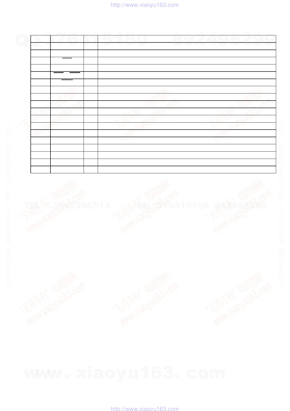
Pin No. Pin Name I/O Description
188 DRVRDY I Ready signal input from the mechanism controller
189 VNW — Power supply terminal (+5V)
190 ALE O Latch enable signal output to the bus interface
191 RST_SPC O Reset signal output to the mechanism controller
192 to 194
HCS3 to HCS1 O Chip select signal output terminal Not used
195 HCS0 O Chip select signal output to the program ROM
196 VDDP — Power supply terminal (+3.3V)
197 TRST O Reset signal output to the DSD decoder (FLX7D only)
198 TDO O Data output to the DSD decoder (FLX7D only)
199 TDI I Data input terminal Not used
200 TMS O Mode selection signal output to the DSD decoder (FLX7D only)
201 TCK O Clock signal output to the DSD decoder (FLX7D only)
202 RESET I Reset signal input from the system controller “L”: reset
203 BUS CLK O Not used
204 GND — Ground terminal
205 VDD — Power supply terminal (+1.8V)
206, 207 HA3, HA2 O Address signal output to the program ROM and bus interface
208 GNDP — Ground terminal
w
w
w
.
x
i
a
o
y
u
1
6
3
.
c
o
m
Q
Q
3
7
6
3
1
5
1
5
0
9
9
2
8
9
4
2
9
8
T
E
L
1
3
9
4
2
2
9
6
5
1
3
9
9
2
8
9
4
2
9
8
0
5
1
5
1
3
6
7
3
Q
Q
TEL 13942296513 QQ 376315150 892498299
TEL 13942296513 QQ 376315150 892498299
http://www.xiaoyu163.com
http://www.xiaoyu163.com
 Loading...