EasyManua.ls Logo

Sony HCD-GPX9 User Manual

Sony HCD-GPX9
72 pages
To Next Page IconTo Next Page
Page #1 background imageLoading...
Page #1 background image
SERVICE MANUAL
COMPACT DISC DECK RECEIVER
AEP Model
UK Model
HCD-GPX9
Ver. 1.1 2005.05
SPECIFICATIONS
9-879-468-02
2005E05-1
© 2005.05
Sony Corporation
Personal Audio Group
Published by Sony Engineering Corporation
– Continued on next page –
HCD-GPX9 is the amplifier, CD player, tape deck
and tuner section in CMT-GPX9DAB.
Model Name Using Similar Mechanism HCD-GPX5
CD
CD Mechanism Type CDM80B-K6BD80A
Section
Base Unit Name BU-K6BD80A
Optical Pick-up Block Name KSM-213DCP
Tape deck
Model Name Using Similar Mechanism HCD-GPX5
Section
Tape Transport Mechanism Type CMAL1Z234A
AUDIO POWER SPECIFICATIONS
Main unit
Amplifier section
DIN power output (rated): 30 + 30 W
(6 ohms at 1 kHz, DIN)
Continuous RMS power output (reference):
35 + 35 W
(6 ohms at 1 kHz, 10%
THD)
Music power output (reference):
60 + 60 W
Inputs
AUDIO IN: Sensitivity 250 mV,
impedance 47 kilohms
Outputs
PHONES: Accepts headphones with
an impedance of 8 ohms or
more
SPEAKER: Accepts impedance of 6 to
16 ohms.
CD player section
Laser Diode Properties
Emission Duration:
Continuous
Laser Output*:
Less than 44.6 µW
µ
*This output is the value measurement at a distance of
200 mm from the objective lens surface on the
Optical Pick-up Block with 7 mm operture.
Frequency response 20 Hz – 20 kHz
Wavelength 780 – 790 nm
Aerial terminal 75 , F female
FM stereo, FM/AM superheterodyne tuner
FM tuner section
Tuning range 87.5 – 108.0 MHz
Aerial FM lead aerial
Aerial terminals 75 ohms unbalanced
Intermediate frequency 10.7 MHz
AM tuner section
Tuning range
531 – 1,602 kHz
(with the tuning interval
set at 9 kHz)
Aerial AM loop aerial, external
aerial terminal
Intermediate frequency 450 kHz
Tape deck section
Recording system 4-track 2-channel, stereo
Frequency response 50 – 13,000 Hz (±3 dB),
using Sony TYPE I
cassettes
Tuner section
DAB tuner section
Frequency range
Band-III: 174.928 (5A) –
239.200 (13F) MHz
L-Band: 1452.960 MHz (L1) –
1490.624 MHz (L23)
(L-Band is not available
for the UK model.)
*For details, see “DAB frequency table” below.
w
w
w
.
x
i
a
o
y
u
1
6
3
.
c
o
m
Q
Q
3
7
6
3
1
5
1
5
0
9
9
2
8
9
4
2
9
8
T
E
L
1
3
9
4
2
2
9
6
5
1
3
9
9
2
8
9
4
2
9
8
0
5
1
5
1
3
6
7
3
Q
Q
TEL 13942296513 QQ 376315150 892498299
http://www.xiaoyu163.com

Table of Contents

Question and Answer IconNeed help?

Do you have a question about the Sony HCD-GPX9 and is the answer not in the manual?

Sony HCD-GPX9 Specifications

General IconGeneral
BrandSony
ModelHCD-GPX9
CategoryStereo System
LanguageEnglish

Summary

SERVICE MANUAL

HCD-GPX9

Service manual title and model number.

AUDIO POWER SPECIFICATIONS

Details on amplifier output power, sensitivity, and impedance.

SPECIFICATIONS

Technical specifications for various sections like frequency response, tuner, etc.

General

Power requirements

Electrical power requirements for the unit.

SAFETY-RELATED COMPONENT WARNING!!

SAFETY-RELATED COMPONENT WARNING!!

Warning about critical components identified by mark.

SECTION 1 SERVICING NOTES

SERVICING NOTES

General notes and precautions for servicing the unit.

SECTION 2 GENERAL

GENERAL

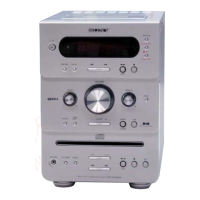
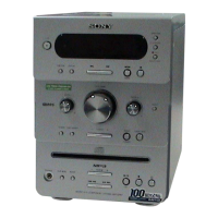
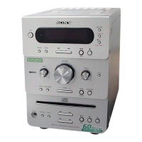
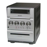
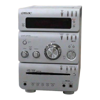
Overview of the unit and location of controls.

List of button locations and reference pages

Map of buttons on the main unit and their corresponding page numbers.

SECTION 3 DISASSEMBLY

DISASSEMBLY

Detailed flow and instructions for disassembling the unit.

3-1. DISASSEMBLY FLOW

Step-by-step flowchart for disassembling the unit.

SECTION 4 TEST MODE

TEST MODE

Procedures for entering and using various test modes.

[MC COLD RESET]

Procedure for cold resetting the unit and clearing preset data.

[COMMON TEST MODE]

Procedure for entering and operating the common test mode.

[PANEL TEST MODE]

Procedure for entering and operating the panel test mode.

Version Check

Procedure to check the software version of various modules.

Key Check

Procedure for checking button inputs and volume/tone control responses.

SECTION 5 ELECTRICAL ADJUSTMENTS

ELECTRICAL ADJUSTMENTS

Procedures for performing electrical adjustments on the unit.

REC BAIS ADJUSTMENT

Procedure for adjusting the record bias for tape playback.

SECTION 6 DIAGRAMS

6-1. BLOCK DIAGRAM - CD SERVO Section -

Block diagram of the CD servo system, detailing signal paths.

SECTION 7 EXPLODED VIEWS

EXPLODED VIEWS

Exploded views of various sections with part references.

SECTION 8 ELECTRICAL PARTS LIST

ELECTRICAL PARTS LIST

Comprehensive list of electrical parts used in the unit.

SERVICING NOTES

NOTES ON HANDLING THE OPTICAL PICK-UP BLOCK OR BASE UNIT

Precautions for handling the optical pick-up block due to electrostatic discharge.

Remote control

ALPHABETICAL ORDER

Alphabetical list of remote control buttons and their functions.

BUTTON DESCRIPTIONS

Detailed descriptions of the remote control buttons.

3-6. MAIN BOARD

3-6. MAIN BOARD

Procedure and diagram for removing the main board.

3-8. CD MECHANISM DECK BLOCK

3-8. CD MECHANISM DECK BLOCK

Procedure and diagram for removing the CD mechanism deck block.

Test Mode Procedures

CD SECTION

Note:

Notes on CD block operation, disc usage, and oscilloscope impedance.

FOCUS BIAS CHECK

Procedure for checking focus bias, especially after replacing the optical block.

RF signal reference waveform (eye pattern)

Reference waveform for RF signal check, showing eye pattern characteristics.

6-2. BLOCK DIAGRAM - AUDIO Section -

6-2. BLOCK DIAGRAM - AUDIO Section -

Block diagram of the audio signal path, including inputs and output.

6-3. BLOCK DIAGRAM - PANEL/POWER SUPPLY Section -

6-3. BLOCK DIAGRAM - PANEL/POWER SUPPLY Section -

Block diagram of the panel and power supply circuits.

6-4. PRINTED WIRING BOARD - DRIVER Board

6-5. SCHEMATIC DIAGRAM - DRIVER Board

6-6. PRINTED WIRING BOARD - BD Board -

6-7. SCHEMATIC DIAGRAM - BD Board -

6-8. PRINTED WIRING BOARD - DAB Board -

6-9. SCHEMATIC DIAGRAM - DAB Board -

6-10. PRINTED WIRING BOARD - MAIN Board -

6-11. SCHEMATIC DIAGRAM - MAIN Section (1/2) -

6-12. SCHEMATIC DIAGRAM - MAIN Section (2/2) -

6-13. SCHEMATIC DIAGRAM - MAIN Section (3/3) -

6-14. PRINTED WIRING BOARD - AMP Board -

6-15. SCHEMATIC DIAGRAM - AMP Board -

6-16. PRINTED WIRING BOARD - PANEL (1) Board -

6-17. SCHEMATIC DIAGRAM - PANEL (1) Board -

6-18. PRINTED WIRING BOARD - PANEL (2) Board -

6-19. SCHEMATIC DIAGRAM - PANEL (2) Board -

6-20. PRINTED WIRING BOARD - POWER Board -

6-21. SCHEMATIC DIAGRAM - POWER Board -

Waveforms

- BD Board -

IC101 CXD3058AR

Pin function description and block diagram for IC101.

- AMP Board -

IC251 BA5947FM-E2

Block diagram and pin description for IC251 on the AMP board.

IC602 RT8H015C-T112-1

Block diagram and pin description for IC602 on the AMP board.

- DAB Board -

IC907 BA50BC0WFP-E2

Block diagram and pin description for IC907 on the DAB board.

IC911 BA33BC0WFP-E2

Block diagram and pin description for IC911 on the DAB board.

- MAIN Board -

IC201 HD14053BFP

Block diagram and pin description for IC201 on the MAIN board.

IC302 BD3402KS2

Block diagram and pin description for IC302 on the MAIN board.

- PANEL (1) Board -

IC801 \u03bcPD16315GB-3BS

Block diagram and pin description for IC801 on the PANEL (1) board.

MAIN BOARD IC306 M30622MEP-A27FPU0 (SYSTEM CONTROLLER)

Pin No.

Description

Description of each pin's function on IC306 (cont.).

7-2. FRONT PANEL SECTION

7-3. TOP BLOCK SECTION

7-4. MAIN SECTION

7-5. CHASSIS SECTION-2

7-6. CD MECHANISM DECK SECTION-1

7-7. CD MECHANISM DECK SECTION-2

7-8. CD MECHANISM DECK SECTION-3

7-9. CD MECHANISM DECK SECTION-4

7-10. BASE UNIT SECTION

AMP BD

DAB DRIVER MAIN

MAIN PANEL (1)

MAIN

PANEL (1) PANEL (2)

POWER

Related product manuals