23
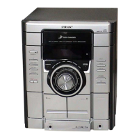
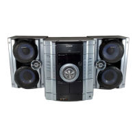
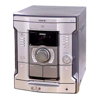
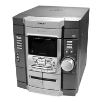
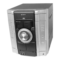
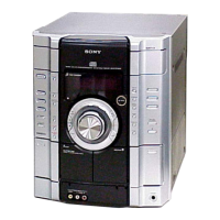
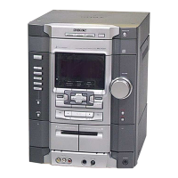
HCD-GX25/RG220
SECTION 5
DIAGRAMS
5-1. IC PIN DESCRIPTIONS
• IC309 BU2099FV (MULTI CONTROLLER) (MAIN BOARD)
Pin No. Pin Name I/O Pin Description
1 VSS — Ground pin
2NC—Not used. (Open)
3DATAISerial data input from the tape mechanism controller
4 CLOCK I Serial data transfer clock signal input from the system controller
5 LCK I Serial data latch pulse clock signal input from the system controller
6 REC O Recording on/off control signal output “L”: recording
7BIAS O Recording bias on/off control signal output “L”: bias on
8A/BO
Deck-A/B selection signal output to the deck-A/B select switch
“L”: deck-B, “H”: deck-A
9 PB MUTE O
Playback muting on/off control signal output to the recording/playback equalizer
amplifier “H”: muting on
10 REC MUTE O
Recording muting on/off control signal output to the recording/playback equalizer
amplifier “L”: muting on
11 TUNER MUTE O Tuner muting on/off control signal output to the tuner unit “H”: muting on
12 LM-R (CD) O Loading motor drive signal output
13 LM-L (CD) O Loading motor drive signal output
14 TM-R (CD) O Table motor drive signal output
15 TM-L (CD) O Table motor drive signal output
16 SP RELAY O Front speaker on/off relay drive control signal output “L”: front speaker on
17 LINK/MATRIX O Surround speaker on/off relay drive control signal output “H”: surround speaker on
18 SO O Serial data output to the bass boost controller
19 OE — Not used. (Connect to ground.)
20 VDD — Power supply pin (+3.3 V)
 Loading...