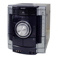
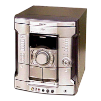
HCD-RV222D/RV222DL/RV333D/RV333DL/RV555D
5
1. SERVICING NOTES ............................................. 6
2. DISASSEMBLY
2-1. Case ................................................................................. 9
2-2. VOL-LED Board ............................................................ 9
2-3. Tuner Assy ...................................................................... 10
2-4. Loading Panel ................................................................. 10
2-5. DVD Block ..................................................................... 11
2-6. Front Panel Section ......................................................... 11
2-7. Back Panel Section ......................................................... 12
2-8. MAIN Board ................................................................... 12
2-9. 2CH-AMP Board (RV222D/RV222DL/RV555D),
3CH-AMP Board (RV333D/RV333DL) ......................... 13
2-10. Tape Mechanism Block................................................... 13
2-11. JACK-MIC AMP Board ................................................. 14
2-12. Lid (TC-L), Lid (TC-R) .................................................. 14
2-13. TC AMP Board ............................................................... 15
2-14. PANEL Board ................................................................. 15
2-15. KEY-RIGHT Board ........................................................ 16
2-16. KEY-LEFT Board ........................................................... 16
2-17. DMB19 Board ................................................................. 17
2-18. Base Unit ......................................................................... 17
2-19. Optical Pick-up ............................................................... 18
2-20. DRIVER Board, SW Board ............................................ 18
2-21. SENSOR Board .............................................................. 19
2-22. MOTOR (TB) Board....................................................... 19
2-23. MOTOR (LD) Board ...................................................... 20
3. TEST MODE ............................................................ 21
4. ELECTRICAL ADJUSTMENTS ........................ 26
5. DIAGRAMS
5-1. Block Diagram –RF Section– ......................................... 28
5-2. Block Diagram –DVD Out Section– .............................. 29
5-3. Block Diagram –Audio Section– .................................... 30
5-4. Block Diagram –Tape Section– ...................................... 31
5-5. Block Diagram –AMP Section– ..................................... 32
5-6. Block Diagram –Power Section– .................................... 33
5-7. Printed Wiring Boards –Driver Section– ........................ 35
5-8. Schematic Diagram –Driver Section– ............................ 36
5-9. Printed Wiring Board –DMB19 Section (1/2)– .............. 37
5-10. Printed Wiring Board –DMB19 Section (2/2)– .............. 38
5-11. Schematic Diagram –DMB19 Section (1/4)– ................. 39
TABLE OF CONTENTS
5-12. Schematic Diagram –DMB19 Section (2/4)– ................. 40
5-13. Schematic Diagram –DMB19 Section (3/4)– ................. 41
5-14. Schematic Diagram –DMB19 Section (4/4)– ................. 42
5-15. Printed Wiring Boards –REG/Tuner Section– ................ 43
5-16. Schematic Diagram –REG Section– ............................... 44
5-17. Schematic Diagram –Tuner Section– ............................. 45
5-18. Printed Wiring Board –Main Section– ............................ 46
5-19. Schematic Diagram –Main Section (1/3)– ...................... 47
5-20. Schematic Diagram –Main Section (2/3)– ...................... 48
5-21. Schematic Diagram –Main Section (3/3)– ...................... 49
5-22. Printed Wiring Board –Jack-MIC AMP Section– ........... 50
5-23. Schematic Diagram –Jack-MIC AMP Section–.............. 51
5-24. Printed Wiring Board –TC AMP Section– ...................... 52
5-25. Schematic Diagram –TC AMP Section– ........................ 53
5-26. Printed Wiring Boards –Panel Section– .......................... 54
5-27. Printed Wiring Boards –Key-Left/Key-Right Section– ... 55
5-28. Schematic Diagram –Panel Section– .............................. 56
5-29. Printed Wiring Board
–2CH-AMP Section (RV222D/RV222DL/RV555D)– ... 57
5-30. Schematic Diagram
–2CH-AMP Section (RV222D/RV222DL/RV555D)– ... 58
5-31. Printed Wiring Board
–3CH-AMP Section (RV333D/RV333DL)– ................... 59
5-32. Schematic Diagram
–3CH-AMP Section (RV333D/RV333DL)– ................... 60
5-33. Printed Wiring Board
–Power Section (RV222D/RV222DL)– .......................... 61
5-34. Schematic Diagram
–Power Section (RV222D/RV222DL)– .......................... 62
5-35. Printed Wiring Board
–Power Section (RV333D/RV333DL/RV555D)–........... 63
5-36. Schematic Diagram
–Power Section (RV333D/RV333DL/RV555D)–........... 64
6. EXPLODED VIEWS
6-1. Overall Section ............................................................... 74
6-2. Front Panel Section-1 ...................................................... 75
6-3. Front Panel Section-2 ...................................................... 76
6-4. Chassis Section ............................................................... 77
6-5. DVD Section ................................................................... 78
6-6. DVD Mechanism Deck Section-1 .................................. 79
6-7. DVD Mechanism Deck Section-2 .................................. 80
7. ELECTRICAL PARTS LIST .............................. 81
Ver. 1.3