58
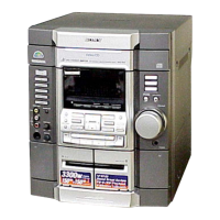
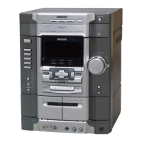
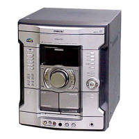
HCD-RV7/RV8
Pin No. Pin Name I/O Description
111 CLOK I
Serial data transfer clock signal input
112 L SENS I
SENS signal input
113 SENS O
SENS signal output
114 L SLCK O
SENS serial data readout clock signal output
115 SCLK I
SENS serial data readout clock signal input
116 VDD3 —
Digital power supply terminal (+2.5V) (for CD-DSP block)
117 ATSK I/O
Input/output terminal for anti-shock Not used
118 XUGF O
XUGF signal output terminal Not used
119 XPCK O
XPCK signal output terminal Not used
120 L GFS I
Guard frame sync signal input
121 GFS O
Guard frame sync signal output
122 VSS3 —
Digital ground terminal
123 L CDC2PO I
C2 pointer signal input
124 C2PO O
C2 pointer signal output
125 L SCOR I
Subcode sync (S0+S1) detection signal input
126 SCOR O
Subcode sync (S0+S1) detection signal output
127 COUT O
Numbers of track counted signal output terminal Not used
128 VDD4 —
Digital ground terminal (for CD-DSP block)
129 MIRR I/O
Mirror signal input/output terminal Not used
130 DFCT I/O
Defect signal input/output terminal Not used
131 L FOK I/O
Focus OK signal input/output
132 FOK I/O
Focus OK signal input/output
133 MDP O
Spindle motor servo drive signal output
134 VSS4 —
Digital ground terminal
135 SSTP I
Detection signal input from limit in switch The optical pick-up is inner position when “H”
136 FSTO O
2/3 frequency-division output of the XTAI (pin <zv. ) Not used
137 SFDR O
Sled motor servo drive signal (+) output
138 SRDR O
Sled motor servo drive signal (–) output
139 VDD5 —
Digital power supply terminal (+2.5V) (for CD-DSP block)
140 TFDR O
Tracking coil servo drive signal (+) output
141 TRDR O
Tracking coil servo drive signal (–) output
142 FFDR O
Focus coil servo drive signal (+) output
143 FRDR O
Focus coil servo drive signal (–) output
144 VSS5 —
Digital ground terminal
145 WFCK O
Write frame clock signal output terminal Not used
146 WDCK O
Word clock signal output terminal Not used
147 ASYE I
Asymmetry circuit on/off control signal input terminal “L”: off, “H”: on Not used
148 VDD6 —
Digital power supply terminal (+2.5V) (for CD-DSP block)
149 XTAI I
Main system clock input terminal (33.8688 MHz)
150 XTAO O
Main system clock output terminal (33.8688 MHz)
151 VSS6 —
Digital ground terminal
152 TES1 I
Input terminal for the test Normally: fixed at “L”
153 TEST I
Input terminal for the test Normally: fixed at “L”
154, 155 RESERVE —
Not used
156 AVD0 —
Analog power supply terminal (+2.5V)
157 IGEN I
Operational amplifier constant current input
w
w
w
.
x
i
a
o
y
u
1
6
3
.
c
o
m
Q
Q
3
7
6
3
1
5
1
5
0
9
9
2
8
9
4
2
9
8
T
E
L
1
3
9
4
2
2
9
6
5
1
3
9
9
2
8
9
4
2
9
8
0
5
1
5
1
3
6
7
3
Q
Q
TEL 13942296513 QQ 376315150 892498299
TEL 13942296513 QQ 376315150 892498299
http://www.xiaoyu163.com
http://www.xiaoyu163.com