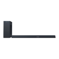
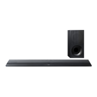
HT-CT770
54
Pin No. Pin Name I/O Description
1 SIRCS_IN I SIRCS signal input from the remote control receiver
2 SIRCS2 I SIRCS signal input from the remote control receiver
3 DSP_MOSI O Serial data output to the serial fl ash and DSP
4 DSP_ MISO I Serial data input from the serial fl ash and DSP
5 DSP_SPICLK O Serial data transfer clock signal output to the serial fl ash and DSP
6 BYTE I External data bus width selection signal input terminal Fixed at “L” in this unit
7 CNVss I Processor mode selection signal input terminal
8 ROM_SDA I/O Two-way data bus with the EEPROM
9 ROM_SCLK O Serial data transfer clock signal output to the EEPROM
10 RESET I
System reset signal input terminal “L”: reset
For several hundreds msec. after the power supply rises, “L” is input, then it change to “H”
11 Xout O System clock output terminal (8 MHz)
12 Vss - Ground terminal
13 Xin I System clock input terminal (8 MHz)
14 Vcc1 - Power supply terminal (+3.3V)
15 CEC_I/O I/O Two-way CEC serial data with the HDMI connector
16 DIR_ZERO I Zero data detection signal input from the digital audio interface receiver
17 RFDET_NFC I Magnetic fi eld detection signal input from the NFC module “L”: magnetic fi eld is detected
18 DRIVE_OCP (DIAG) I Shut down signal input from the digital power amplifi er “L”: shut down
19 WL_DET O Not used
20 BT_LED O LED drive signal output terminal for the lamp (blue) “H”: LED on
21 WL_RST O Reset signal output to the RF modulator “L”: reset
22 N.A O Not used
23 HDMI_TX_5VPWR O
+5V power on/off control signal output terminal for the TV (ARC) HDMI OUT connector
“H”: power on
24 HDMI_NON_LPCM O Audio setting signal output terminal “L”: LPCM audio, “H”: HBR audio
25 DIR_ERROR I Error detection signal input from the digital audio interface receiver “L”: error
26 PCONT_DRIVER O Power on/off control signal output terminal for the digital power amplifi er “H”: power on
27 DAMP_SCL O Serial data transfer clock signal output to the stream processor
28 DAMP_SDA I/O Two-way data bus with the stream processor
29 M_TX_OUT O Serial data output to the DSP
30 M_RX_IN I Serial data input from the DSP
31 SCD/CLK1 I Serial data transfer clock signal input terminal for fl ash writing
32 RTS1/MC_BT_CTS0 I Clear to send signal input from the Bluetooth module
33 MC_BT_TXD0 O Serial data output to the Bluetooth module
34 MC_BT_RXD0 I Serial data input from the Bluetooth module
35 N.A O Not used
36 MC_BT_RTS O Return to send signal output to the Bluetooth module
37 P_CONT2 O Power on/off control signal output terminal “H”: power on
38 A_SEL0 O Analog audio selection signal output terminal “L”: external analog input, “H”: Bluetooth
39 HOLD I Fixed at “L” in this unit
40 WL_SCL O I2C clock signal output to the RF modulator
41 WL_SDA I/O Two-way I2C data bus with the RF modulator
42 BT_RST O Reset signal output to the Bluetooth module “L”: reset
43 PCONT_BT O +3.3V power on/off control signal output terminal for the Bluetooth section “H”: power on
44 WR I Fixed at “H” in this unit
45 HDMI_SDA I/O Two-way I2C data bus with the HDMI transceiver
46 HDMI_SCL O I2C clock signal output to the HDMI transceiver
47 HDMI_MUTE_DET I HDMI muting on/off control signal input from the HDMI transceiver “H”: muting on
48 DSP_SPIDS O Chip select signal output to the serial fl ash and DSP
49 DSP_RESET O Reset signal output to the DSP “L”: reset
50 SF_HOLD_DSP O Hold signal output to the serial fl ash “L”: hold
51 DIR_HCE O Chip enable signal output to the digital audio interface receiver
52 DIR_XSTATE I Source clock selection monitor input from the digital audio interface receiver
53 DIR_RST O Reset signal output to the digital audio interface receiver “L”: reset
54 HDMI_RST O Reset signal output to the HDMI transceiver “H”: reset
55 HDMI_MUTE_ON O HDMI muting on/off control signal output terminal “H”: muting on
56 HDMI_INT I Interrupt signal input from the HDMI transceiver
57 SEL_HDMI O HDMI selection signal output terminal “H”: HDMI
MAIN BOARD IC1002 R5F3650RDFB#30 (SYSTEM CONTROLLER)