– 19 – – 20 –
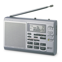
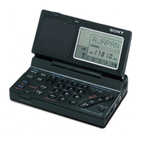
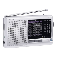
ICF-SW35
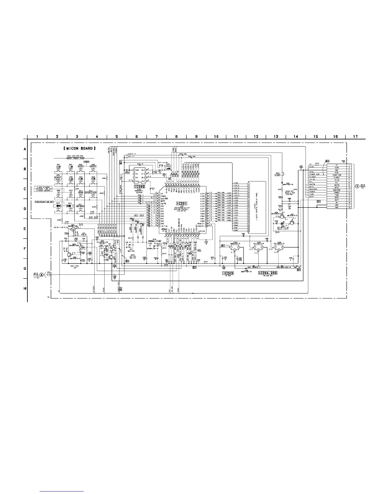
Note on Schematic Diagram:
• All capacitors are in µF unless otherwise noted. pF: µµF
50 WV or less are not indicated except for electrolytics
and tantalums.
• All resistors are in Ω and
1
/
4
W or less unless otherwise
specified.
•
f
: internal component.
• C : panel designation.
• U : B+ Line.
• H : adjustment for repair.
• Power voltage is dc 4.5 V and fed with regulated dc power
supply from battery terminal.
• Voltage is dc with respect to ground under no-signal
(detuned) condition.
no mark : FM
( ) : MW/LW
< > : SW
4-6. SCHEMATIC DIAGRAM — MICON SECTION — • Refer to page 21 for IC Block Diagrams.
(Page 15)
(Page 15)