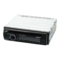
MEX-BT4100E/BT4100P/BT4100U/BT4150U
44
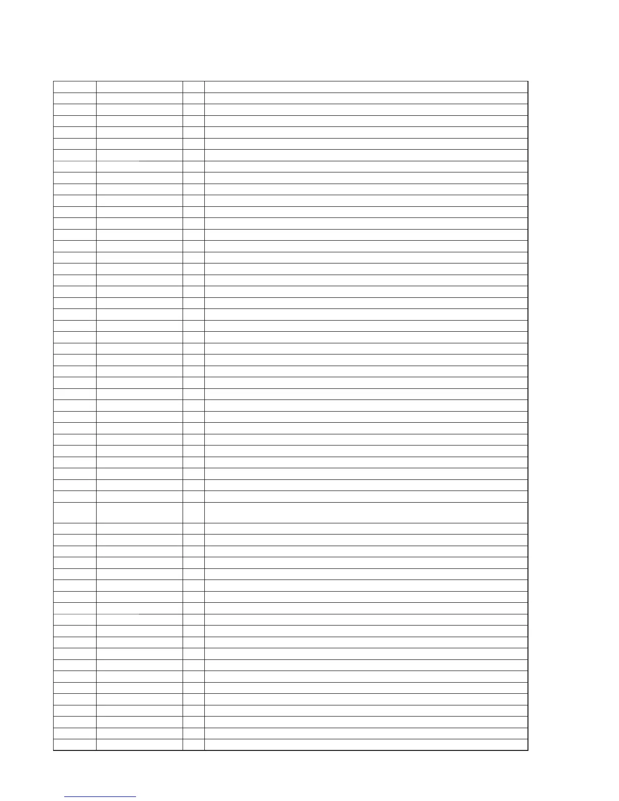
MAIN BOARD IC601 TMPM320C1DFG-9999 (SUB SYSTEM CONTROLLER)
Pin No. Pin Name I/O Description
1 MODE1 I Operation mode setting terminal Fixed at “L” in this unit
2 RESETn I Reset signal input terminal from the main system controller
3 DRV_ON O Driver control signal output to the CD section
4 BSIF_INT I Request signal input from the audio DSP
5 DEC_INT I Request signal input from the audio DSP
6 (DOOR_SW) - Not used
7 MEC_LIMIT I Detection signal input from the CD section (limit switch)
8 CD_XRST O Reset request signal output to the main system controller “L”: reset
9 DEC_XMUTE O Muting on/off control signal output to the audio DSP
10 SF_WP O Write protect signal output to the serial fl ash
11 SF_HOLD O Hold signal output to the serial fl ash
12 DVCC3.3IO - Power supply terminal (+3.3V)
13 DVSSCOM - Ground terminal
14 SP_CLK O Spectrum analyzer data transfer clock signal output to the audio DSP
15 SP_DATA I Spectrum analyzer data input from the audio DSP
16 CD_ZDET I Zero detection signal input from the audio DSP
17 A-ATT O Muting on/off control signal output to the main system controller
18 SF_SO O Serial data output to the serial fl ash
19 SF_SI I Serial data input from the serial fl ash
20 SF_CE O Chip enable signal output to the serial fl ash
21 SF_CLK O Serial data transfer clock signal output to the serial fl ash
22 BSIF_DATA O Audio data output to the audio DSP
23 BSIF_GATE O Gate signal output to the audio DSP
24 BSIF_LRCK O L/R sampling clock signal output to the audio DSP
25 BSIF_BCK O Bit clock signal output to the audio DSP
26 LCD_DO O Serial data output to the liquid crystal display driver
27 ILL_IN I Illuminate line detect signal input terminal
28 LCD_CE O Chip enable signal output to the liquid crystal display driver
29 LCD_CLK O Serial data transfer clock signal output to the liquid crystal display driver
30 DVCC3.3IO - Power supply terminal (+3.3V)
31 DVSSCOM - Ground terminal
32 DVCC1.2DRM - Power supply terminal (+1.2V)
33 DVCC1.2DRM - Power supply terminal (+1.2V)
34 DVSSCOM - Ground terminal
35 SWDCK O Debug terminal (for ICE) Not used
36 SWDIO I/O Debug terminal (for ICE) Not used
37 to 40
CD_BUS0 to
CD_BUS3
O Serial data output to the audio DSP
41 CD_BUCK O Serial data transfer clock signal output to the audio DSP
42 DVCC33IO - Power supply terminal (+3.3V)
43 DVCC3.3DRM - Power supply terminal (+3.3V)
44 DVSSCOM - Ground terminal
45 CD_XCCE O Chip enable signal output to the audio DSP
46 USB_EN - Not used
47 CP_SEL I EEPROM setting terminal “H”: EEPROM use
48 DVCC1.2 - Power supply terminal (+1.2V)
49 BT_TX O Serial data output to the Bluetooth section
50 BT_RX I Serial data input from the Bluetooth section
51 BT_CTS I Clear to send signal input from the Bluetooth section
52 BT_RTS O Return to send signal output to the Bluetooth section
53 DVSS_COM - Ground terminal
54 BT_POWER O Power supply on/off control signal output terminal for the Bluetooth section “H”: power on
55 BT_RESET O Reset signal output to the Bluetooth section “L”: reset
56 BT_MIC_DET I Bluetooth microphone detection signal input terminal “L”: microphone is connected
57 CP_RESET O Reset signal output terminal Not used
58 MC_TX O Serial data output to the main system controller
59 MC_RX I Serial data input from the main system controller
60 I2C_SCL O Serial data transfer clock signal output to the EEPROM