3
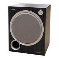
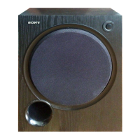
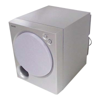
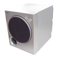
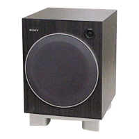
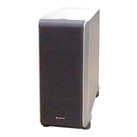
SA-WMS356/WMS556
SECTION 1
DIAGRAMS
For Schematic Diagrams.
Note:
• All capacitors are in µF unless otherwise noted. (p: pF)
50 WV or less are not indicated except for electrolytics and
tantalums.
• All resistors are in Ω and
1
/
4
W or less unless otherwise
specified.
• f : internal component.
• C : panel designation.
• A : B+ Line.
• B : B– Line.
•Voltages and waveforms are dc with respect to ground un-
der no-signal (detuned) conditions.
no mark: Power on
•Voltages are taken with a VOM (Input impedance 10 MΩ).
Voltage variations may be noted due to normal production
tolerances.
• Signal path.
F : AUDIO
For Printed Wiring Boards.
Note:
• X : parts extracted from the component side.
• Y : parts extracted from the conductor side.
• : Pattern from the side which enables seeing.
THIS NOTE IS COMMON FOR PRINTED WIRING BOARDS AND SCHEMATIC DIAGRAMS.
(In addition to this, the necessary note is printed in each block.)
Note: The components identified by mark 0 or dotted
line with mark 0 are critical for safety.
Replace only with part number specified.
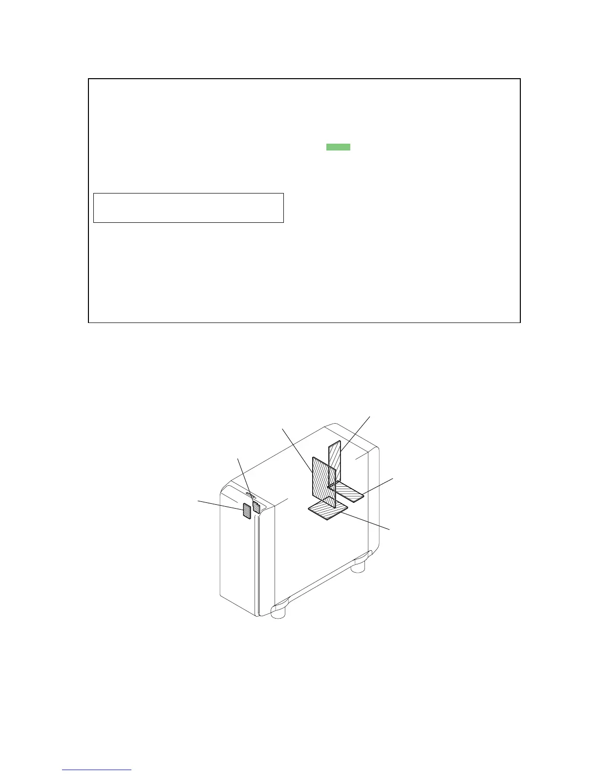
LED board
MAIN board
CONTROL board
POWER AMP board
POWER SUPPLY board
POWER SWITCH board
NOTE FOR PRINTED WIRING BOARDS AND SCHEMATIC DIAGRAMS
• Circuit Boards Location