4
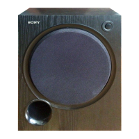
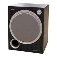
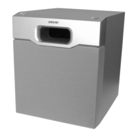
SA-WMSP69
• NOTE FOR PRINTED WIRING BOARDS AND SCHEMATIC DIAGRAMS
• A : B+ Line.
• B : B– Line.
•Voltages are dc with respect to ground under no-signal
(detuned) conditions.
no mark : Power on
•Voltages are taken with a VOM (Input impedance 10 MΩ).
Voltage variations may be noted due to normal production
tolerances.
• Signal path.
F : AUDIO
THIS NOTE IS COMMON FOR PRINTED WIRING
BOARDS AND SCHEMATIC DIAGRAMS.
(In addition to this, the necessary note is
printed in each block.)
For schematic diagrams:
Note:
• All capacitors are in µF unless otherwise noted. (p: pF)
50 WV or less are not indicated except for electrolytics
and tantalums.
• All resistors are in Ω and
1
/
4
W or less unless otherwise
specified.
• C : panel designation.
Note: The components identified by mark 0 or dotted line
with mark 0 are critical for safety.
Replace only with part number specified.
For printed wiring boards:
Note:
• X : parts extracted from the component side.
• Y : parts extracted from the conductor side.
•: Pattern from the side which enables seeing.