EasyManua.ls Logo

Sony SCD-XA777ES Service Manual

Sony SCD-XA777ES
137 pages
To Next Page IconTo Next Page
Page #1 background imageLoading...
Page #1 background image
SERVICE MANUAL
Model Name Using Similar Mechanism NEW
CD Mechanism Type
CDM19JB-DVBU4B
CDM19JN-DVBU4B
Base Unit Name DVBU4B
Optical Pick-up Name KHM-230AAA
SUPER AUDIO CD PLAYER
US Model
Canadian Model
AEP Model
SPECIFICATIONS
SCD-XA777ES
Ver 1.1 2001.10
9-873-192-02 Sony Corporation
2001J0500-1 Home Audio Company
C 2001.10 Published by Sony Engineering Corporation
(US and Canadian models)
When a super audio CD is played
Playing frequency range 2 Hz to 100 kHz
Frequency response 2 Hz to 50 kHz (–3 dB)
Dynamic range 108 dB or more
Total harmonic distortion rate
0.0012 % or less
Wow and flutter Value of measurable limit (±0.001 %
W. PEAK) or less
When a CD is played
Frequency response 2 Hz to 20 kHz
Dynamic range 100 dB or more
Total harmonic distortion rate
0.0017 % or less
Wow and flutter Value of measurable limit (±0.001 %
W. PEAK) or less
Output connector
*Output only the audio signals of the CD
Laser radiant power: 5.47 uW at 650 nm
*These output is the value measured at a distance of about
200mm from the objective lens surface on the optical pick-up.
Power requirements 120 V AC, 60 Hz
230 V AC, 50/60 Hz (AEP model)
Power consumption 32 W
Dimensions (w/h/d) 430 × 130 × 380 mm
(17 × 5 1/8 × 15 in.)
incl. projecting parts
Mass (approx.) 16 kg (35 lbs 5 oz.)
Supplied accessories
Design and specifications are subject to change without notice.
ANALOG OUT
DIGITAL (CD)
OUT
OPTICAL*
DIGITAL (CD)
OUT
COAXIAL*
PHONES
Jack type
Phono
jacks
Square
optical
output
connector
Coaxial
output
connector
Stereo
phone jack
Output level
2 Vrms
(at 50 kilohms)
–18 dBm
0.5 Vp-p
10 mW
Load impedance
Over 10 kilohms
Light emitting
wave length:
660 nm
75 ohms
32 ohms
( )
Audio connecting cord
phono jack × 2 (Red and White) y phono jack × 2 (Red
and White) (3)
phono jack × 1 (Black) y phono jack × 1 (Black) (2)
Remote commander RM-SX700 (1)
R06 (size-AA) batteries (2)
AC power cord (Mains lead) (1)
General
Laser Semiconductor laser
(SACD: λ = 650 nm)
(CD: λ = 780 nm)
Emission duration: continuous

Table of Contents

Other manuals for Sony SCD-XA777ES

Question and Answer IconNeed help?

Do you have a question about the Sony SCD-XA777ES and is the answer not in the manual?

Sony SCD-XA777ES Specifications

SACD Playback IconSACD Playback
playback frequency range2Hz - 100kHz
frequency response2Hz - 50kHz (-3dB)
dynamic rangeMore than 108dB
harmonic distortionLess than 0.0018%
wow and flutterBelow Measurement Limit (±0.001% W-Peak)
CD Playback IconCD Playback
dac converterSuper Audio D/A
frequency response2Hz - 20kHz (± 0.5dB) (EIAJ)
dynamic rangeMore than 99dB
harmonic distortionLess than 0.0020% (EIAJ)
wow and flutterBelow Measurement Limit (±0.001% W-Peak)
Outputs IconOutputs
total output level digital optical-18dB (fix)
total output level digital coaxial0.5Vp-p (fix)
total output level analog unbalance2Vrms (fix)
total output level headphone10mW
Power IconPower
power requirementsAC120V, 60Hz
power consumption38W
Weight and Dimensions IconWeight and Dimensions
dimensions17" x 5.4" x 16.1"
weight35 lbs.

Summary

SPECIFICATIONS

When a super audio CD is played

Details audio performance metrics when playing Super Audio CDs.

When a CD is played

Details audio performance metrics when playing standard CDs.

Output connector

Lists available audio output connectors for analog and digital signals.

General

Provides general specifications and features of the player.

SAFETY CHECK-OUT

LEAKAGE TEST

Details the method for checking AC leakage current from exposed metal parts.

CAUTION

Notes on chip component replacement

Flexible Circuit Board Repairing

SERVICING NOTES

MODEL IDENTIFICATION

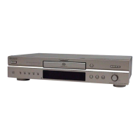
Describes how to identify the model based on the back panel information.

NOTES ON HANDLING THE OPTICAL PICK-UP BLOCK OR BASE UNIT

Offers precautions for handling sensitive optical pick-up and base unit components.

NOTES ON LASER DIODE EMISSION CHECK

Provides safety instructions for checking laser diode emissions.

CLEANING OF OPTICAL PICK-UP LENS

Recommends using an air blower for cleaning the optical pick-up lens.

RESETTING OPERATION AT POWER ON

Details the power-on sequence with a disc loaded.

HOW TO OPEN THE DISC TABLE WHEN POWER SWITCH TURNS OFF

OPTICAL PICK-UP SERVICE POSITION

D-POWER/POWER BOARDS AND RF BOARD SERVICE POSITION

MAIN BOARD SERVICE POSITION

AUDIO MODULE BLOCK SERVICE POSITION

NOTE FOR INSTALLATION (AUDIO MODULE BLOCK)

NOTE ON POSITION OF WIRE (FLAT TYPE)

GENERAL

Front Panel Parts Descriptions

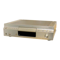
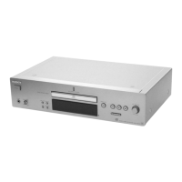
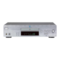
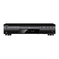
Identifies and describes controls and indicators on the front panel.

Rear Panel Parts Descriptions

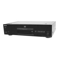
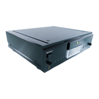
Identifies and describes connectors and ports on the rear panel.

Remote Parts Descriptions

Identifies and describes the functions of the remote control buttons.

DISASSEMBLY

3-1. DISASSEMBLY FLOW

Outlines the sequence of disassembly steps for the unit.

3-2. CASE (TOP)

Instructions for removing the top case of the unit.

3-3. LOADING PANEL ASSY

Instructions for removing the disc loading mechanism.

3-4. FRONT PANEL SECTION

Instructions for removing the front panel assembly.

3-5. MAIN BOARD, BRACKET (MAIN)

Instructions for removing the main board and its associated bracket.

3-6. MECHANISM DECK (CDM19JB-DVBU4B/CDM19JN-DVBU4B), RF BOARD

Instructions for removing the mechanism deck and RF board unit.

3-7. DISC TABLE, BELT, LOADING MOTOR (M1)

Instructions for removing the disc table, belt, and loading motor.

3-8. OPTICAL PICK-UP (KHM-230AAA/J1NP)

Instructions for removing the optical pick-up assembly.

3-9. BASE UNIT (DVBU4B)

Instructions for removing the base unit assembly.

TEST MODE

FLUORESCENT INDICATOR TUBE MODE

Describes the test mode for checking the fluorescent display tube and IC communication.

Test Mode Command List

FOCUS command (2X)

OFFSET (PI, FE, TE) command (3X)

TRACKING command (4X)

SEARCH command (5X)

DISC DETECT command (6X)

TOOLS command (8X)

QA command (9X)

How to Apply Servo by Manual Operation

Set Check

Manual Check Method

Provides detailed steps for performing individual checks within the manual test mode.

4-1. IC AND FLUORESCENT DISPLAY TUBE CHECK (SELF-DIAGNOSIS)

4-2. AUTO CHECK (AUTOMATIC VARIOUS MEASUREMENTS)

CD and SACD (SL) Disc Operation Check

Details the procedure for checking the operational stability with CD and SACD single layer discs.

4-3. SACD (DL) DISC OPERATION CHECK

4-4. HYBRID DISC OPERATION CHECK

4-5. AGING MODE

4-5-1. The aging can be performed to the set in the test mode

Explains how aging tests are conducted and repeated until completion or error.

4-6. SHIPPING MODE

Error List

< How to view the error history >

Provides instructions on how to access and review the recorded error history.

4-7. WAVEFORMS CHECK

BU Electrical Adjustment Mode

Details the mode for electrical adjustments related to waveforms.

S Curve Check

Procedure for checking the S curve waveform output.

Traverse Check

Procedure for checking the traverse waveform output.

RF Level Check

CLV Jitter Check (CD only)

Checking and Connecting Location

DIAGRAMS

5-1. BLOCK DIAGRAM – RF/SERVO Section –

Block diagram illustrating the RF and servo control sections.

5-2. BLOCK DIAGRAM – MAIN Section (1/2) –

5-3. BLOCK DIAGRAM – MAIN Section (2/2) –

5-4. BLOCK DIAGRAM – AUDIO Section (1/2) –

5-5. BLOCK DIAGRAM – AUDIO Section (2/2) –

5-6. BLOCK DIAGRAM – DISPLAY/POWER SUPPLY Section –

NOTE FOR PRINTED WIRING BOARDS AND SCHEMATIC DIAGRAMS

Note on Printed Wiring Board

Explains the conventions and symbols used in printed wiring board diagrams.

Note on Schematic Diagram

Explains the conventions and symbols used in schematic diagrams.

Circuit Boards Location

Illustrates the physical location of various circuit boards within the unit.

5-8. PRINTED WIRING BOARDS – LOADING MOTOR/RF/SWITCH Boards –

5-9. SCHEMATIC DIAGRAM – LOADING MOTOR/RF/SWITCH Boards –

5-10. PRINTED WIRING BOARD – MAIN Board (Component Side) –

5-11. PRINTED WIRING BOARD – MAIN Board (Conductor Side) –

5-12. SCHEMATIC DIAGRAM – MAIN Board (1/5) –

5-13. SCHEMATIC DIAGRAM – MAIN Board (2/5) –

5-14. SCHEMATIC DIAGRAM – MAIN Board (3/5) –

5-15. SCHEMATIC DIAGRAM – MAIN Board (4/5) –

5-16. SCHEMATIC DIAGRAM – MAIN Board (5/5) –

5-17. PRINTED WIRING BOARD – D.OUT Board –

5-18. SCHEMATIC DIAGRAM – D.OUT Board –

5-19. PRINTED WIRING BOARD – MOTHER Board (Component Side) –

5-20. PRINTED WIRING BOARD – MOTHER Board (Conductor Side) –

5-21. SCHEMATIC DIAGRAM – MOTHER Board (1/2) –

5-22. SCHEMATIC DIAGRAM – MOTHER Board (2/2) –

5-23. PRINTED WIRING BOARD – AUDIO FRONT Board –

5-24. SCHEMATIC DIAGRAM – AUDIO FRONT Board –

5-25. PRINTED WIRING BOARD – AUDIO SURR Board –

5-26. SCHEMATIC DIAGRAM – AUDIO SURR Board –

5-27. PRINTED WIRING BOARD – AUDIO C/SW Board –

5-28. SCHEMATIC DIAGRAM – AUDIO C/SW Board –

5-29. PRINTED WIRING BOARD – PANEL Board –

5-30. SCHEMATIC DIAGRAM – PANEL Board –

5-31. PRINTED WIRING BOARDS – HP/JOG/KEY/R.CNTL Boards –

5-32. SCHEMATIC DIAGRAM – HP/JOG/KEY/R.CNTL Boards –

5-33. PRINTED WIRING BOARD – A-POWER Board –

5-34. SCHEMATIC DIAGRAM – A-POWER Board –

5-35. PRINTED WIRING BOARD – D-POWER Board –

5-36. SCHEMATIC DIAGRAM – D-POWER Board –

5-37. PRINTED WIRING BOARDS – AC/AC SW Boards –

5-38. SCHEMATIC DIAGRAM – AC/AC SW Boards –

• Waveforms – RF Board –

IC001 el (TE) (CD PLAY)

Waveform example for IC001 TE signal during CD playback.

IC001 el (FE) (CD PLAY)

Waveform example for IC001 FE signal during CD playback.

IC001 tj (RFAC) (CD PLAY)

Waveform example for IC001 RFAC signal during CD playback.

• Waveforms – MAIN Board –

IC803 ia (A1)

Waveform example for IC803 A1 signal.

IC803 uk (A2)

Waveform example for IC803 A2 signal.

IC811 1

Waveform example for IC811 signal.

IC901 ra (EXTAL)

Waveform example for IC901 EXTAL signal.

IC509 el (FE) (CD PLAY)

Waveform example for IC509 FE signal during CD playback.

qs IC509 el (FE) (SACD PLAY)

qd IC509 ra (TE) (CD PLAY)

qf IC509 ra (TE) (SACD PLAY)

qg IC509 t; (RFAC) (CD PLAY)

qh IC509 t; (RFAC) (SACD PLAY)

– MOTHER Board –

– PANEL Board –

w; IC1001 ea (EXTAL)

Waveform example for IC1001 EXTAL signal.

• IC Block Diagrams

IC001 CXD1881R (RF Board)

Block diagram for IC001, the RF board's CXD1881R integrated circuit.

IC101, 201 CXD9657N/2K (AUDIO FRONT Board)

IC303 HD74LV161ATELL (MOTHER Board)

IC304, 305, 306, 307, 308 HD74LV157ATELL (MOTHER Board)

IC509 CXD3008Q (MAIN Board)

IC701 CXD1882R-1 (MAIN Board)

IC904 BU2500FV-E2 (MAIN Board)

IC905 M51957BFP-600C (MAIN Board)

IC1002 MSM9201-03GS-K (PANEL Board)

5-39. IC PIN FUNCTION DESCRIPTION

• MAIN BOARD IC701 CXD1882R-1 (SACD DECODER)

• MAIN BOARD IC801 CXD2752R (DSD DECODER)

• MAIN BOARD IC803 CXD9647R (DSD DIGITAL SIGNAL PROCESSOR)

• MAIN BOARD IC901 CXP973F064R-1 (CPU)

• MAIN BOARD IC902 CXD1095BR (I/O EXPANDER)

SECTION 6 EXPLODED VIEWS

6-1. CASE SECTION

Exploded view of the unit's case assembly and related parts.

6-2. FRONT PANEL SECTION

6-3. BOTTOM SECTION

6-4. BOARD SECTION-1

6-5. BOARD SECTION-2

6-6. CHASSIS SECTION

6-7. MECHANISM DECK SECTION (CDM19JB-DVBU4B, CDM19JN-DVBU4B)

6-8. BASE UNIT SECTION (DVBU4B)

SECTION 7 ELECTRICAL PARTS LIST

AC

Electrical parts list for the AC board.

A-POWER

Electrical parts list for the A-POWER board.

D-POWER

Electrical parts list for the D-POWER board.

AC SW

Electrical parts list for the AC SW board.

Related product manuals