Do you have a question about the Sony SCD-XA9000ES and is the answer not in the manual?
| CD-R playback | Yes |
|---|
| Depth | 380 mm |
|---|---|
| Width | 430 mm |
| Height | 130 mm |
| Weight | 16000 g |
Details performance metrics for Super Audio CD playback, including frequency range and distortion.
Details performance metrics for standard CD playback, including frequency response and dynamic range.
Specifies the data transmission speed, protocol, and format for the i.LINK connection.
Details the types, output levels, and load impedance of the unit's output connectors.
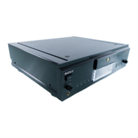
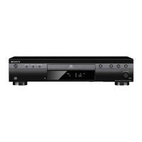
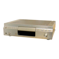
Provides general specifications for laser type, power requirements, dimensions, and mass.
Lists similar mechanism types and model identification for different regions.
Lists the items provided with the Super Audio CD player.
Details the safety check process, including methods for measuring AC leakage current.
Precautions for handling the optical pick-up and ensuring laser safety during operation.
Guidelines for replacing chip components and repairing flexible circuit boards.
Information regarding the use of unleaded solder and the lead-free mark indication.
Identifies different model versions based on back panel markings.
Precautions for handling the optical pick-up block and laser diode emission.
Describes the sequence of operations performed at power-on for different disc types.
Step-by-step instructions on how to open the disc table when the power is off.
Procedure for positioning the optical pick-up for servicing.
Illustrates the service position for removing D-POWER, POWER, and RF boards.
Specific instructions for connecting flat wires to the RF board.
Setup instructions for checking the main board, including required jigs.
Procedure for servicing the front panel section.
Illustrates the correct placement for servicing the audio module block.
Important guidance on how to properly install the audio module block.
Warning about keeping flat wires clear of high-temperature heatsinks.
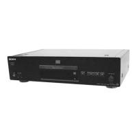
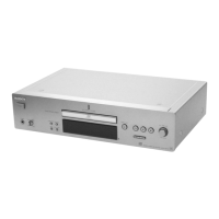
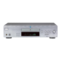
Descriptions of POWER switch, disc tray, Play, Pause, and Stop buttons.
Details on PHONES, PHONE LEVEL, SACD/CD, MULTI/2CH, and MENU controls.
Information on the display window, remote sensor, and AMS dial functions.
Details on ANALOG 5.1CH OUT, DIGITAL (CD) OUT, and ANALOG 2CH OUT jacks.
Description of the i.LINK S200 AUDIO OUT jack and AC IN terminal.
Notes on the i.LINK indicator status and signal output behavior.
Descriptions of CONTINUE, SHUFFLE, PROGRAM, DISPLAY MODE, REPEAT, and AyB buttons.
Details on Number buttons, >10, AMS, m/M, and INDEX buttons for track selection.
Functions of SACD/CD, MULTI/2CH, ENTER, CLEAR, LEVEL ADJ, and CHECK buttons.
Visual representation of the sequence for disassembling the unit.
Detailed steps for removing the top case and side plates.
Instructions for detaching the loading panel assembly.
Steps to disconnect and remove the front panel section.
Instructions for removing the main board and its associated bracket.
Procedures for detaching the RF board and the mechanism deck assembly.
Steps for removing the disc table, drive belt, and loading motor.
Detailed instructions for removing the optical pick-up module.
Steps for removing the base unit assembly from the chassis.
Instructions on how to enter and exit the diagnostic test mode.
Explanation of the command structure for test mode operations.
Specifies the necessary discs for performing various test mode checks.
Commands for tracking servo adjustment, track search, and disc type detection.
Commands for laser control, aging, and general diagnostic tools.
Commands for quality assurance checks and IC interface communication.
Step-by-step guide for manually applying servo functions for analysis.
Procedure to verify communication between the microcomputer and main ICs.
List of error displays and their common causes for IC interface issues.
Steps to perform automatic operational stability checks and measurements.
List of items measured during SET CHECK and their specified OK/NG values.
Detailed numerical specifications for measured items used in OK/NG judgments.
Guidance on comparing hexadecimal measurement values against specifications.
Procedure to check the stability of dual-layer SACD playback.
Instructions for initializing the set to shipping mode after repair.
Instructions for performing checks on S-curve, traverse, and RF waveforms.
Methods for analyzing CLV jitter, RF level, and traverse waveforms.
Procedure to confirm i.LINK connection and bus reset functionality.
Schematic showing signal flow within the RF and servo circuitry.
Illustration of signal paths within the main section of the circuitry.
Continuation of the main section's signal path diagram.
Diagram illustrating the signal paths for audio processing.
Continuation of the audio signal path illustration.
Schematic showing the signal paths for the i.LINK interface.
Diagram illustrating the front panel controls and power supply circuitry.
Guidelines for understanding symbols and notations on PWB diagrams.
Guidelines for interpreting symbols and notations in schematic diagrams.
Visual reference showing the physical location of various circuit boards.
Diagram illustrating the physical layout of the servo section's printed wiring board.
Detailed electrical schematic diagram of the servo section.
Diagram showing component placement on the main board's component side.
Diagram showing the circuit traces on the main board's conductor side.
First part of the electrical schematic for the main board.
Second part of the electrical schematic for the main board.
Third part of the electrical schematic for the main board.
Fourth part of the electrical schematic for the main board.
Fifth part of the electrical schematic for the main board.
Sixth part of the electrical schematic for the main board.
Final part of the electrical schematic for the main board.
Diagram showing the physical layout of the D-OUT board.
Electrical schematic diagram for the D-OUT board.
Diagram showing component placement on the mother board's component side.
Diagram showing the circuit traces on the mother board's conductor side.
First part of the electrical schematic for the mother board.
Second part of the electrical schematic for the mother board.
Diagram showing the physical layout of the audio front board.
Electrical schematic diagram for the audio front board.
Diagram showing the physical layout of the audio surround board.
Electrical schematic diagram for the audio surround board.
Diagram showing the physical layout of the audio center/subwoofer board.
Electrical schematic diagram for the audio center/subwoofer board.
First part of the electrical schematic for the i.LINK interface.
Second part of the electrical schematic for the i.LINK interface.
Diagram showing the physical layout of the i.LINK interface board.
Layout diagrams for the display, jog, key, and HP boards.
First part of the electrical schematic for the panel controls.
Second part of the electrical schematic for the panel controls.
Diagram showing component placement on the A-POWER board's component side.
Diagram showing circuit traces on the A-POWER board's conductor side.
Layout diagrams for the IC boards.
Electrical schematic diagrams for the A-POWER and IC boards.
Illustrative waveforms captured from the RF board.
Illustrative waveforms captured from the main board.
Illustrative waveforms from the link and display boards.
Diagram showing component placement on the D-POWER board's component side.
Diagram showing circuit traces on the D-POWER board's conductor side.
Electrical schematic diagram for the D-POWER board.
Diagram showing component placement on the AC board's component side.
Diagram showing circuit traces on the AC board's conductor side.
Diagram showing the physical layout of the AC SW board.
Electrical schematic diagrams for the AC and AC SW boards.
Illustrative waveforms captured from Mother, Link, and Display boards.
Block diagrams illustrating the functionality of key ICs on the RF board.
Description of the pins for the CXD3068Q IC on the main board.
Description of the pins for the TMC57929PGF-RDP IC (SACD Decoder).
Includes diagrams and pinout details for multiple integrated circuits.
Continuation of pin descriptions for the CXD3068Q IC.
Further continuation of pin descriptions for the CXD3068Q IC.
Continuation of pin descriptions for the TMC57929PGF-RDP IC.
Further continuation of pin descriptions for the TMC57929PGF-RDP IC.
Further continuation of pin descriptions for the TMC57929PGF-RDP IC.
Final pin descriptions for the TMC57929PGF-RDP IC.
Description of the pins for the CXD2753R IC (DSD Decoder).
Continuation of pin descriptions for the CXD2753R IC.
Further continuation of pin descriptions for the CXD2753R IC.
Description of the pins for the CXD9722TQ IC (DSD Digital Signal Processor).
Continuation of pin descriptions for the CXD9722TQ IC.
Description of the pins for the CXP973064-241R IC (CPU).
Continuation of pin descriptions for the CXP973064-241R IC.
Description of the pins for the ISPLSI2032VE IC (I/O Expander).
Description of the pins for the TMS320VC5409 IC (i.LINK DSP).
Continuation of pin descriptions for the TMS320VC5409 IC.
Final pin descriptions for the TMS320VC5409 IC.
Description of the pins for the M30626FHPFP IC (i.LINK System Controller).
Continuation of pin descriptions for the M30626FHPFP IC.
Description of the pins for the CXP84120-092Q IC (Display Controller).
Visual breakdown of the unit's case components.
Exploded view illustrating components of the front panel section 1.
Exploded view illustrating components of the front panel section 2.
Exploded view illustrating components of the unit's bottom section.
Exploded view of main, A-POWER, D-OUT, and LINK boards.
Exploded view of D-POWER, MOTHER, and AUDIO boards.
Exploded view illustrating the components of the chassis.
Detailed exploded view of the mechanism deck components.
Exploded view illustrating the components of the base unit.
List of electrical components for the AC and AC SW boards.
List of electrical components for the D-POWER board.
List of electrical components for the audio front and surround boards.
List of electrical components for the audio C/SW and front boards.
List of electrical components for the audio surround board.
Continuation of the electrical component list for the audio surround board.
List of electrical components for the display board.
List of electrical components for the D-OUT board.
Continuation of the electrical component list for the D-POWER board.
List of components for jog, key, link, and other interface/control boards.
List of components for the link, loading motor, and main boards.
List of resistors used on the main board.
List of capacitors used on the main board.
List of connectors, diodes, and other components for the main board.
List of resistors used on the main board.
List of resistors used on the main board.
List of resistors used on the main board.
List of components for the main and mother boards.
List of capacitors and connectors for the mother board.
List of diodes, resistors, and other components for the mother board.
List of parts for the RF, SW, and Main boards.
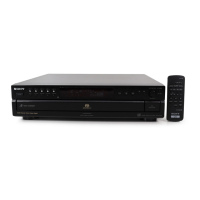
List of items included with the product, including remote commander and manuals.
Records of revisions made to the service manual, including dates and descriptions.