6
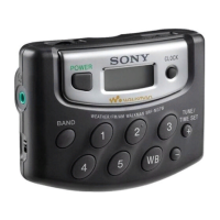
SRF-M37
SECTION 4
DIAGRAMS
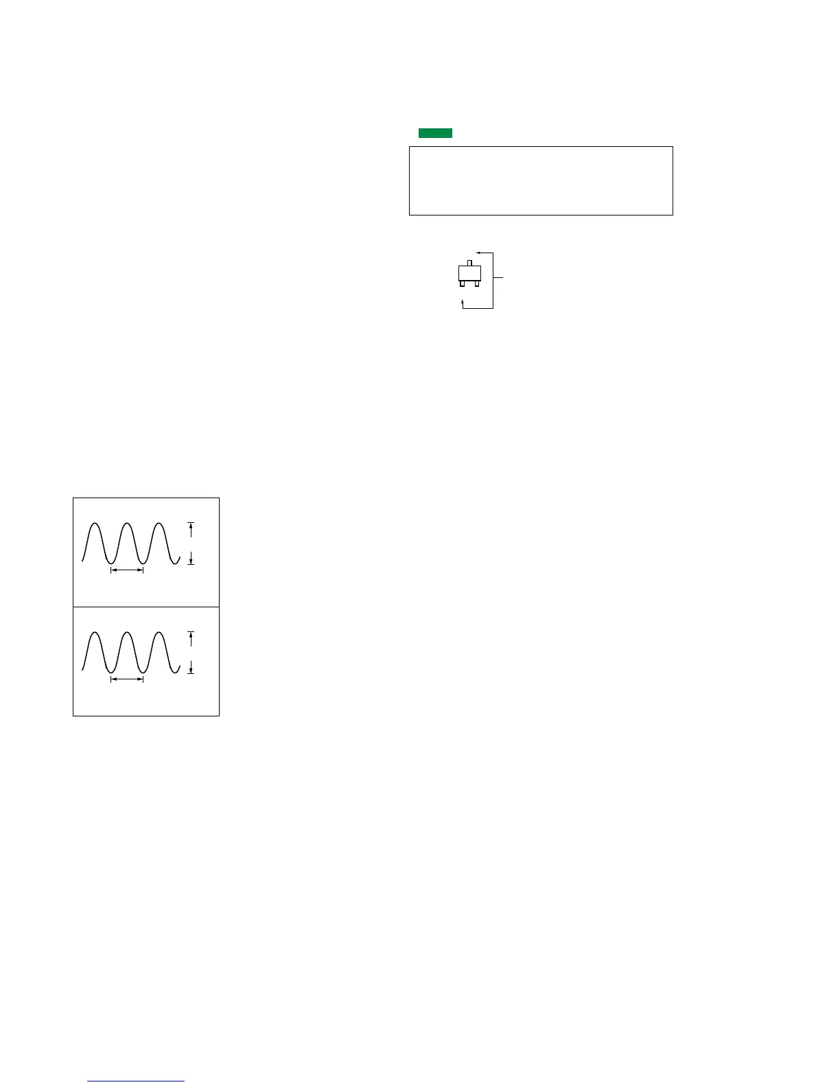
1
IC101 tg XOUT
1.1 Vp-p
13
µ
s
TIME/div :
4 µs/DIV
VOLT/div : 500 mV/DIV
2
Q106 collector
1.8 Vp-p
262 ns
TIME/div :
100 ns/DIV
VOLT/div : 500 mV/DIV
Note on Schematic Diagram:
• All capacitors are in µF unless otherwise noted. pF: µµF
50 WV or less are not indicated except for electrolytics
and tantalums.
• All resistors are in Ω and
1
/
4
W or less unless otherwise
specified.
• C : panel designation.
• A : B+ Line.
• H : adjustment for repair.
•Power voltage is dc 1.5 V and fed with regulated dc power
supply from battery terminal.
•Voltages and waveforms are dc with respect to ground
under no-signal (detuned) conditions.
no mark : FM
<>: AM
•Voltages are taken with a VOM (Input impedance 10 MΩ).
Voltage variations may be noted due to normal produc-
tion tolerances.
•Waveforms are taken with a oscilloscope.
Voltage variations may be noted due to normal produc-
tion tolerances.
• Circled numbers refer to waveforms.
• Signal path.
F : FM
f : AM
• Waveform
Note on Printed Wiring Board:
• Y : parts extracted from the conductor side.
• b : Pattern from the side which enables seeing.
• : Carbon pattern.
Caution:
Pattern face side: Parts on the pattern face side seen from
(Side B) the pattern face are indicated.
Parts face side: Parts on the parts face side seen from
(Side A) the parts face are indicated.
• Indication of transistor