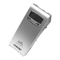
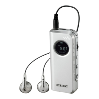
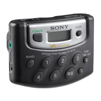
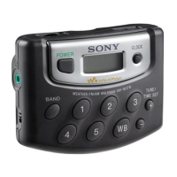
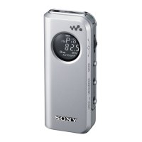
13
SRF-M97
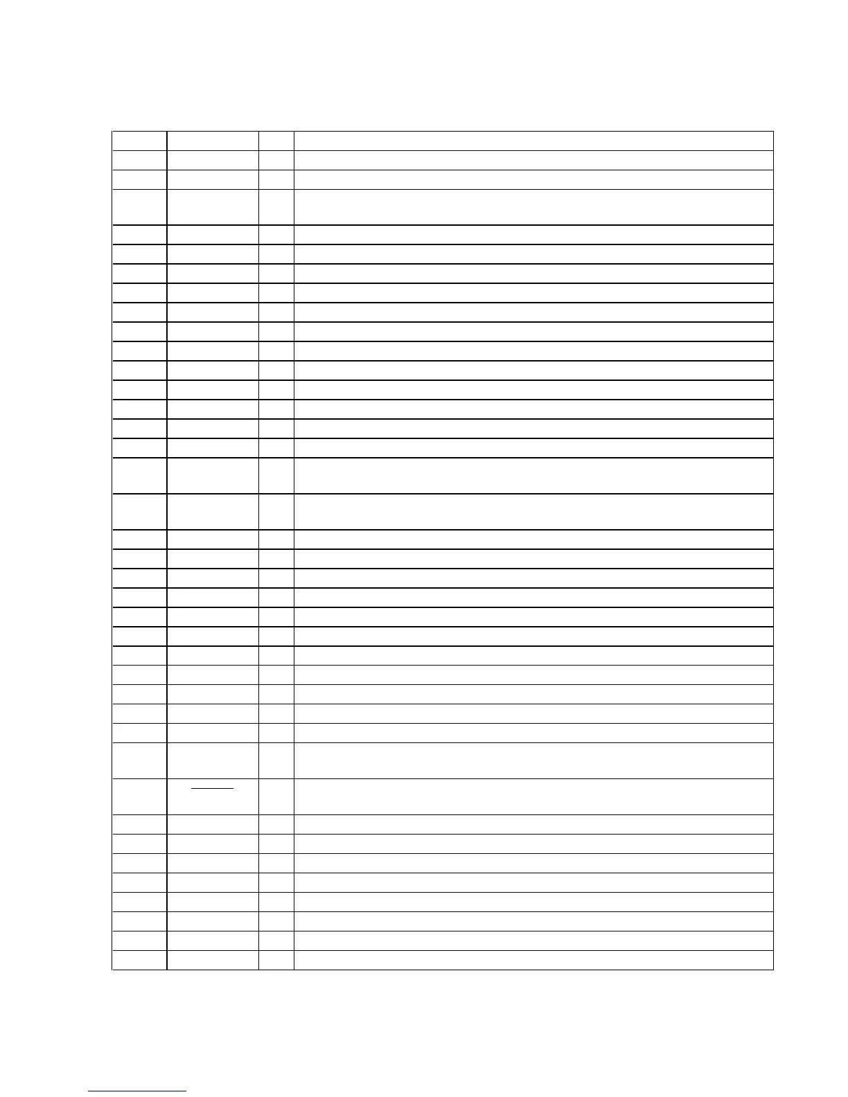
• IC Pin Function Description
MAIN BOARD IC101 TC9329AFAG-609 (S.D) (SYSTEM CONTROLLER)
Pin No. Pin Name I/O Description
1 to 4 COM1 to COM4 O
Common drive signal output to the liquid crystal display
5 to 16 S1 to S12 O
Segment drive signal output to the liquid crystal display
17 SIMUKE1 I
Setting terminal for the destination
"L": Except US and tourist model, "H": US and tourist model
18 SIMUKE2 I
Setting terminal for the destination "L": Except US model, "H": US model
19, 20 P9-0, P9-1 I
Not used
21, 22
KS1, KS2 O Key source signal output to the key matrix
23 to 25
KR1 to KR3 I Key return signal input from the key matrix
26
HOLD SW I HOLD switch input terminal "L": hold on
27
VDD - Power supply terminal (+1.5V)
28
BEEP O Beep signal output terminal
29
MONO/ST O Mono/stereo selection signal output terminal "L": stereo, "H": mono
30
AM BAND O AM band selection signal output terminal "H": AM
31
DDCON O DC/DC converter on/off control signal output terminal "L": DC/DC converter on
32
BAND2 O Band selection signal output terminal "L": FM, "H": AM
33 TEST I
Test mode control signal input terminal Not used
34
INT2 I
Battery detection signal input terminal
"L": battery mark residual quantity less display lights up
35
INT1 I
1.0V voltage detection signal input terminal
"L": battery mark residual quantity less display lights up
36
IF IN2 I IF pulse signal input terminal Not used
37
GND - Ground terminal
38
OSC IN I VCO input from the FM/AM front-end
39
VDD - Power supply terminal (+1.5V)
40 D0 O
Phase comparator output terminal
41
VREG - Constant voltage power supply output terminal for the phase comparator (+1.5V)
42 to 45
P3-0 to P3-3 I Not used
46 to 49
P5-0 to P5-3 I Not used
50
MUTE O Muting on/off control signal output to the headphone power amplifier "L": muting on
51
POWER ON O Power supply on/off control signal output terminal "L": power on
52
BAND1 O Band selection signal output terminal "L": AM, "H": FM
53
AMP ON O
Audio amplifier on/off control signal output to the headphone power amplifier
"H": Audio amplifier on
54 RESET I
System reset signal input from the reset signal generator "L": reset For several
hundreds msec. after the power supply rises, "L" is input, then it changes to "H"
55
XOUT O System clock output terminal (75 kHz)
56
XIN I System clock input terminal (75 kHz)
57
GND - Ground terminal
58
VDB - Terminal for power supply voltage pressure up
59, 60 C1, C2 -
Connection terminal of the capacitor for power supply voltage pressure up
61 VEE -
Constant voltage power supply output terminal for the liquid crystal display drive (+1.5V)
62, 63 C3, C4 -
Connection terminal of the capacitor for liquid crystal display drive voltage pressure up
64 VCLD -
Liquid crystal display drive voltage power supply output terminal
Ver. 1.1