33
STR-DE197
STR-DE197
TABLE OF CONTENTS
1. Printed Wiring Boards –Main Section–................................... 4
2. Schematic Diagram –Main Section (1/2)– .............................. 5
3. Schematic Diagram –Main Section (2/2)– .............................. 6
4. Printed Wiring Boards –Panel Section– .................................. 7
5. Schematic Diagram –Panel Section–....................................... 8
6. Electrical Parts List.................................................................. 9
THIS NOTE IS COMMON FOR PRINTED WIRING
BOARDS AND SCHEMATIC DIAGRAMS.
(In addition to this, the necessary note is
printed in each block.)
for schematic diagram:
• All capacitors are in µF unless otherwise noted. (p: pF)
50 WV or less are not indicated except for electrolytics
and tantalums.
• All resistors are in Ω and
1
/
4
W or less unless otherwise
specified.
•
f
: internal component.
• 2 : nonflammable resistor.
• 1 : fusible resistor.
• C : panel designation.
• A : B+ Line.
• B : B– Line.
•Voltage and waveforms are dc with respect to ground
under no-signal (detuned) conditions.
no mark : FM
•Voltages are taken with a VOM (Input impedance 10 MΩ).
Voltage variations may be noted due to normal produc-
tion tolerances.
•Waveforms are taken with a oscilloscope.
Voltage variations may be noted due to normal produc-
tion tolerances.
• Circled numbers refer to waveforms.
• Signal path.
F : TUNER (FM/AM)
L : VIDEO (AUDIO)
J : CD (ANALOG)
• Abbreviation
CND : Canadian model.
• (( )): Page of Supplement-1.
for printed wiring boards:
• X : parts extracted from the component side.
•
f
: internal component.
• : Pattern from the side which enables seeing.
• Abbreviation
CND : Canadian model.
• (( )): Page of Supplement-1.
Note:
The components identi-
fied by mark 0 or dotted
line with mark 0 are criti-
cal for safety.
Replace only with part
number specified.
Note:
Les composants identifiés par
une marque 0 sont critiques
pour la sécurité.
Ne les remplacer que par une
piéce portant le numéro
spécifié.
C
B
These are omitted.
E
Q
B
These are omitted.
C
Q
Q
E
BCE
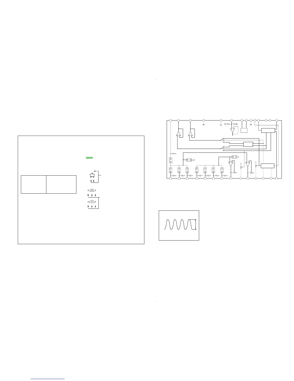
• IC Block Diagram
IC402 R2S15904SP
24 23 22
MCU
I/F
TONE CONTROL
L-CH BASS/TREBLE
SURROUND
21 2025262728
INR4
LOUT
ROUT
AGND
VCC
REFIN
DATA
CLK
DGND
TRER
TREL
NC
BASSL2
NC
INR3
INPUT
SELECTOR
INPUT
SELECTOR
INPUT GAIN
CONTROL
INPUT GAIN
CONTROL
MUTE
MUTE
REF
MODE
SELECTOR
VOLUME
VOLUME
INR2
INR1
INL1
INL2
INL3
INL4
IGOUTL
VOLINL
IGOUTR
VOLINR
BASSR1
BASSL1
BASSR2
19 18 17 16 15
1 2 3 5 6 7 8 94 10 11 12 13 14
TONE CONTROL
R-CH BASS/TREBLE
• Waveform
3.6 Vp-p
2V/DIV, 0.2
µ
sec/DIV
4.19 MHz
1 IC201 eg (X2)