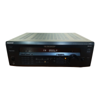
Do you have a question about the Sony STR-DE197 and is the answer not in the manual?
Details on power output and total harmonic distortion for various models.
Technical specifications related to the FM tuner section of the receiver.
Technical specifications related to the AM tuner section of the receiver.
General specifications including power consumption, dimensions, and accessories.
Procedures and methods for testing AC leakage from exposed metal parts.
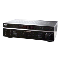
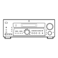
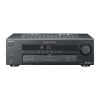
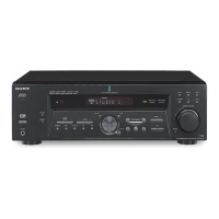
Identification of different models based on part numbers found on the back panel.
Step-by-step instructions for disassembling the case of the unit.
Instructions for disassembling the front panel section.
Instructions for disassembling the back panel of the unit.
Instructions for disassembling the main board.
Guide to locate buttons on the main unit and their corresponding reference pages.
Instructions on initial setup and basic usage of the remote control.
Description and functions of individual buttons on the remote control.
Procedure to test all segments of the fluorescent indicator tube.
Procedure for auto-scanning and memorizing RDS stations.
Method to select the AM tuning interval step (9 kHz or 10 kHz).
Procedure to display the software version and area.
Detailed pin descriptions for IC201 (System Controller).
Diagram illustrating the location of various circuit boards within the unit.
Block diagram illustrating the main section of the receiver's circuitry.
Block diagram illustrating the power section of the receiver's circuitry.
Printed wiring board layout for the main section of the unit.
Schematic diagram for the main section, part 1 of 2.
Schematic diagram for the main section, part 2 of 2.
Printed wiring board layouts for the panel sections (Display, Power, etc.).
Schematic diagrams for the panel sections (Display, Volume, etc.).
Block diagrams illustrating the internal logic of key ICs used in the unit.
Exploded view of the case section, showing all component parts and their assembly.
Exploded view of the front panel section, detailing its components and assembly.
Exploded view of the chassis section, showing internal component layout and assembly.
List of electrical parts for the AC Outlet Board.
List of connectors and vacuum fluorescent display parts.
List of integrated circuits, coils, capacitors, transistors, and resistors.
List of resistors, switches, and vibrator components for display and function key boards.
List of connectors, jacks, capacitors for the H.PHONE board.
List of connectors, jacks, coils, transistors, and resistors for the main board.
List of resistors for the main board, continuing from previous page.
Parts list for power board, transformer, terminal, connectors, diodes, transistors, and resistors.
Parts list for volume board components: connectors, resistors, encoder, and switches.
List of switches for volume board, miscellaneous items, and accessories.
Identifies changes to the MAIN board, listing former and new part numbers.
Identifies changes to the DISPLAY board, listing former and new part numbers.
Details changes for Volume, H. Phone, Power, Function Key, and AC Outlet boards.
| Channel Power Rating | 100W x 2 (8 ohms, 40 Hz - 20kHz, THD 0.09%) |
|---|---|
| Sound Fields | Yes |
| RCA Audio Inputs | 4 (Rear) |
|---|---|
| RCA Audio Outputs | 2 (Rear) |
| AC Outlet | 1 Switched |
| Antenna Terminal (AM Loop) | 1 (Rear) |
| Antenna Terminal (FM 75 Ohm) | 1 (Rear) |
| Headphone Output | 1 (Front) |
| Power Requirements | AC120V, 60 Hz |
|---|---|
| Power Consumption (in Operation) | 190W |
| Power Consumption (in Standby) | 0.5W |
| Weight | 15 lbs 7 oz (7kg) |
|---|---|
| Measurements | 16 13/14" x 5 3/14" x 11 8/9" (430 x 132.5 x 302mm) |