1313
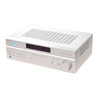
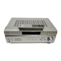
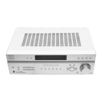
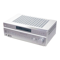
STR-K685
STR-K685
• Circuit Boards Location
SECTION 4
DIAGRAMS
For Schematic Diagrams.
Note:
• All capacitors are in µF unless otherwise noted. (p: pF)
50 WV or less are not indicated except for electrolytics and
tantalums.
• All resistors are in Ω and
1
/
4
W or less unless otherwise
specified.
• % : indicates tolerance.
• f : internal component.
• 2 : nonflammable resistor.
• 5 : fusible resistor.
• C : panel designation.
• A : B+ Line.
• B : B– Line.
•Voltages and waveforms are dc with respect to ground un-
der no-signal (detuned) conditions.
No mark : FM
•Voltages are taken with a VOM (Input impedance 10 MΩ).
Voltage variations may be noted due to normal production
tolerances.
•Waveforms are taken with a oscilloscope.
• Circled numbers refer to waveforms.
• Signal path.
F : FM
J : ANALOG
c : DIGITAL
• Abbreviation
AR : Argentine model
E51 : Chilean and Peruvian models
MX : Mexican model
SP : Singapore model
SP6 : Singapore and Malaysia models
TH : Thai model
For Printed Wiring Boards.
Note:
• X : parts extracted from the component side.
•
a
: Through hole.
• f : internal component.
• : Pattern from the side which enables seeing.
• Indication of transistor.
Caution:
Pattern face side: Parts on the pattern face side seen from
(Side B) the pattern face are indicated.
Parts face side: Parts on the parts face side seen from
(Side A) the parts face are indicated.
C
B
These are omitted.
E
Q
B
These are omitted.
CE
THIS NOTE IS COMMON FOR PRINTED WIRING BOARDS AND SCHEMATIC DIAGRAMS.
(In addition to this, the necessary note is printed in each block.)
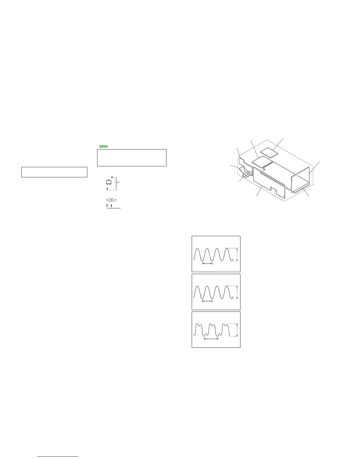
•Waveforms
– DIGITAL Board –
1
IC1905
9
(MCLK1)
1 V/DIV, 40 ns/DIV
72 ns
3.5 Vp-p
2
IC1101
id
(X1)
1 V/DIV, 20 ns/DIV
41.6 ns
4.2 Vp-p
3
IC1301
ws
(XIN)
1 V/DIV, 40 ns/DIV
81.4 ns
4.2 Vp-p
Note: The components identified by mark 0 or dotted
line with mark 0 are critical for safety.
Replace only with part number specified.
DIGITAL board
MAIN board
DISPLAY board
HEADPHONE board
POWER board
DCAC board
STANDBY board
AC SELECT board (E51)
Ver. 1.2