SECTION 3
DIAGRAMS
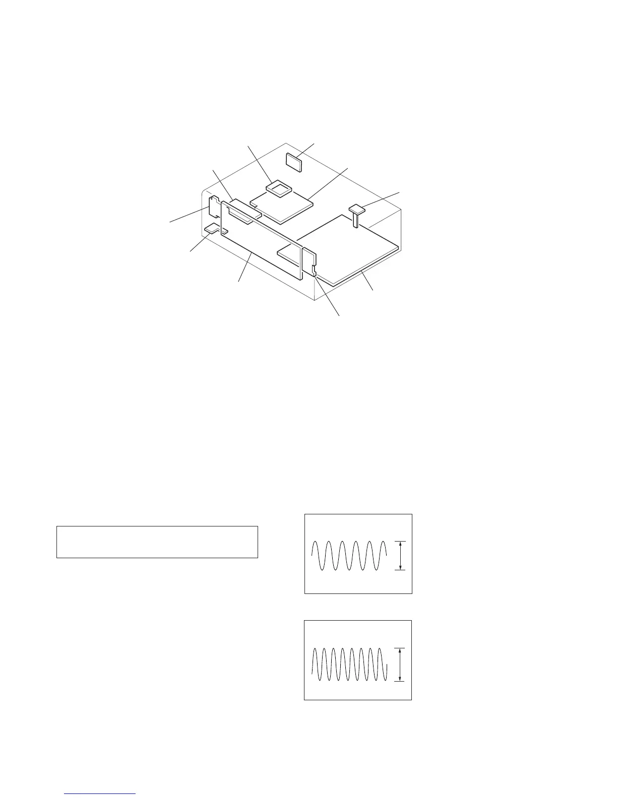
3-1. CIRCUIT BOARDS LOCATION
TRANS 1 board
OUTLET board (AEP, SP, AUS Model)
TRANS 2 board
SW board
HP board
DISPLAY board
VOL board
MAIN board
POWER board
REAR SP board
4
For Schematic Diagrams.
Note:
• All capacitors are in µF unless otherwise noted. pF:
µµF 50 WV or less are not indicated except for
electrolytics and tantalums.
• All resistors are in Ω and
1
/
4
W or less unless otherwise
specified.
• % : indicates tolerance.
•
¢ : internal component.
• 2 : nonflammable resistor.
• 1 : fusible resistor.
• C : panel designation.
• U : B+ Line.
• V : B– Line.
• H : adjustment for repair.
• Voltages and waveforms are dc with respect to ground
under no-signal (detuned) conditions.
No mark : FM
• Voltages are taken with a VOM (Input impedance
10MΩ).
Voltage variations may be noted due to normal
production tolerances.
• Waveforms are taken with a oscilloscope.
• Circled numbers refer to waveforms.
• Signal path.
F : FM
• Abbreviation
AUS : Australian model.
SP : Singapore model.
THIS NOTE IS COMMON FOR PRINTED WIRING
BOARDS AND SCHEMATIC DIAGRAMS.
(In addition to this necessary note is printed in each
block.)
For Printed Wiring Boards.
Note:
• X : parts extracted from the component side.
•
® : Through hole.
•
¢ : internal component.
• b : Pattern from the side which enables seeing.
• Waveform
• DISPLAY SECTION
1
IC401 #∞ (X2)
5.8Vp-p
5MHz
• MAIN SECTION
2
IC300 $§ (OSC)
4.0Vp-p8.0MHz
Note : The components identified by mark ! or dotted
line with mark ! are critical for safety.
Replace only with part number specified.
 Loading...